|
|
|
PDF AD630 Data sheet ( Hoja de datos )
| Número de pieza | AD630 | |
| Descripción | Balanced Modulator/Demodulator | |
| Fabricantes | Analog Devices | |
| Logotipo | ||
Hay una vista previa y un enlace de descarga de AD630 (archivo pdf) en la parte inferior de esta página. Total 8 Páginas | ||
|
No Preview Available !
a
Balanced Modulator/Demodulator
FEATURES
Recovers Signal from +100 dB Noise
2 MHz Channel Bandwidth
45 V/s Slew Rate
–120 dB Crosstalk @ 1 kHz
Pin Programmable Closed Loop Gains of ؎1 and ؎2
0.05% Closed Loop Gain Accuracy and Match
100 V Channel Offset Voltage (AD630BD)
350 kHz Full Power Bandwidth
Chips Available
PRODUCT DESCRIPTION
The AD630 is a high precision balanced modulator which com-
bines a flexible commutating architecture with the accuracy and
temperature stability afforded by laser wafer trimmed thin-film
resistors. Its signal processing applications include balanced
modulation and demodulation, synchronous detection, phase
detection, quadrature detection, phase sensitive detection,
lock-in amplification and square wave multiplication. A network
of on-board applications resistors provides precision closed loop
gains of ± 1 and ± 2 with 0.05% accuracy (AD630B). These
resistors may also be used to accurately configure multiplexer
gains of +1, +2, +3 or +4. Alternatively, external feedback may
be employed allowing the designer to implement his own high
gain or complex switched feedback topologies.
The AD630 may be thought of as a precision op amp with two
independent differential input stages and a precision comparator
which is used to select the active front end. The rapid response
time of this comparator coupled with the high slew rate and fast
settling of the linear amplifiers minimize switching distortion. In
addition, the AD630 has extremely low crosstalk between chan-
nels of –100 dB @ 10 kHz.
The AD630 is intended for use in precision signal processing
and instrumentation applications requiring wide dynamic range.
When used as a synchronous demodulator in a lock-in amplifier
configuration, it can recover a small signal from 100 dB of inter-
fering noise (see lock-in amplifier application). Although optimized
for operation up to 1 kHz, the circuit is useful at frequencies up
to several hundred kilohertz.
Other features of the AD630 include pin programmable frequency
compensation, optional input bias current compensation resis-
tors, common-mode and differential-offset voltage adjustment,
and a channel status output which indicates which of the two
differential inputs is active. This device is now available to Stan-
dard Military Drawing (DESC) numbers 5962-8980701RA and
5962-89807012A.
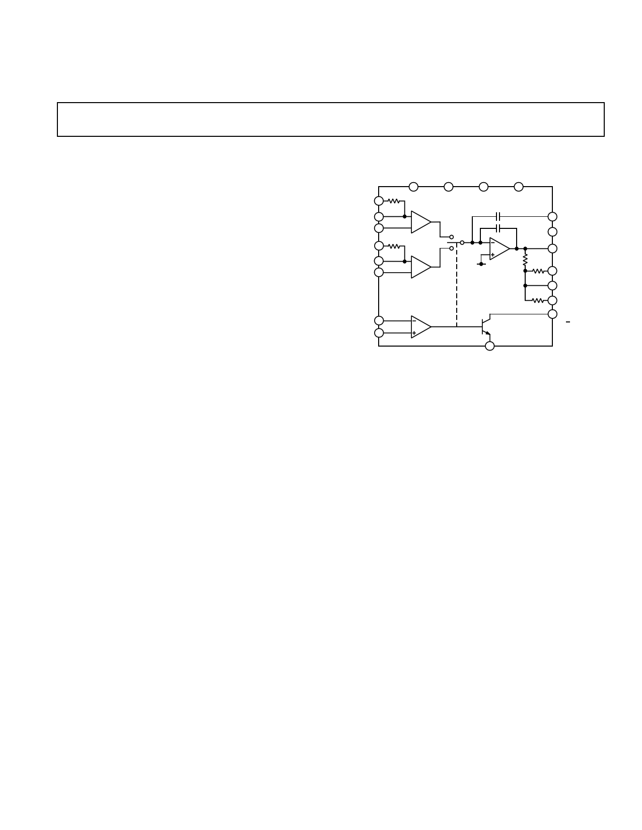
AD630
FUNCTIONAL BLOCK DIAGRAM
CM OFF CM OFF
ADJ
ADJ
2.5k⍀
RINA 1
6
AMP A
5
CHA+ 2
CHA– 20
2.5k⍀
RINB 17
CHB+ 18
A
AMP B B
CHB– 19
DIFF OFF DIFF OFF
ADJ
ADJ
43
AD630
12 COMP
11 +VS
13 VOUT
10k⍀
10k⍀
–V 14 RB
SEL B 9
SEL A 10
COMP
15 RF
5k⍀
16 RA
7
CHANNEL
STATUS
B/A
8
–VS
PRODUCT HIGHLIGHTS
1. The configuration of the AD630 makes it ideal for signal
processing applications such as: balanced modulation and
demodulation, lock-in amplification, phase detection, and
square wave multiplication.
2. The application flexibility of the AD630 makes it the best
choice for many applications requiring precisely fixed gain,
switched gain, multiplexing, integrating-switching functions,
and high-speed precision amplification.
3. The 100 dB dynamic range of the AD630 exceeds that of any
hybrid or IC balanced modulator/demodulator and is compa-
rable to that of costly signal processing instruments.
4. The op-amp format of the AD630 ensures easy implementa-
tion of high gain or complex switched feedback functions.
The application resistors facilitate the implementation of
most common applications with no additional parts.
5. The AD630 can be used as a two channel multiplexer with
gains of +1, +2, +3 or +4. The channel separation of
100 dB @ 10 kHz approaches the limit which is achievable
with an empty IC package.
6. The AD630 has pin-strappable frequency compensation (no
external capacitor required) for stable operation at unity gain
without sacrificing dynamic performance at higher gains.
7. Laser trimming of comparator and amplifying channel offsets
eliminates the need for external nulling in most cases.
REV. C
Information furnished by Analog Devices is believed to be accurate and
reliable. However, no responsibility is assumed by Analog Devices for its
use, nor for any infringements of patents or other rights of third parties
which may result from its use. No license is granted by implication or
otherwise under any patent or patent rights of Analog Devices.
One Technology Way, P.O. Box 9106, Norwood, MA 02062-9106, U.S.A.
Tel: 781/329-4700 World Wide Web Site: http://www.analog.com
Fax: 781/326-8703
© Analog Devices, Inc., 2000
1 page 
AD630
RA
5k⍀
Vi
RB
10k⍀
RF 10k⍀
RF
VO = – RA Vi
Figure 12. Inverting Gain Configuration
Vi
RA
5k⍀
VO = (1+
RF
RB
)
Vi
RB
10k⍀
RF
10k⍀
faster the output signal will move. This feature helps insure
rapid, symmetric settling when switching between inverting and
noninverting closed loop configurations.
The output section of the AD630 includes a current mirror-load
(Q24 and Q25), an integrator-voltage gain stage (Q32), and
complementary output buffer (Q44 and Q74). The outputs of
both transconductance stages are connected in parallel to the
current mirror. Since the deselected input stage produces no
output current and presents a high impedance at its outputs,
there is no conflict. The current mirror translates the differential
output current from the active input transconductance amplifier
into single ended form for the output integrator. The comple-
mentary output driver then buffers the integrator output pro-
duce a low impedance output.
Figure 13. Noninverting Gain Configuration
CIRCUIT DESCRIPTION
The simplified schematic of the AD630 is shown in Figure 14.
It has been subdivided into three major sections, the comparator,
the two input stages and the output integrator. The comparator
consists of a front end made up of Q52 and Q53, a flip-flop load
formed by Q3 and Q4, and two current steering switching cells
Q28, Q29 and Q30, Q31. This structure is designed so that a
differential input voltage greater than 1.5 mV in magnitude
applied to the comparator inputs will completely select one the
switching cells. The sign of this input voltage determine which
of the two switching cells is selected.
+VS 11
SEL A
10 Q52
9
SEL B
CH A–
20
Q33
i55
Q53 Q62
Q28
CH A+ CH B+
2 19
Q34 Q35
Q65 Q67
Q30
Q29
Q31
Q24
CH B–
18
Q36
i73
Q44
Q70
13 VO
C121
Q74
12
C122
Q32
COMP
Q25
Q3 Q4 i22
i23
–VS 8
34
56
DIFF
OFF ADJ
DIFF
OFF ADJ
CM CM
OFF ADJ OFF ADJ
Figure 14. AD630 Simplified Schematic
The collectors of each switching cell connect to an input trans-
conductance stage. The selected cell conveys bias currents i22
and i23 to the input stage it controls, causing it to become active.
The deselected cell blocks the bias to its input stage which, as a
consequence, remains off.
The structure of the transconductance stages is such that they
present a high impedance at their input terminals and draw no
bias current when deselected. The deselected input does not
interfere with the operation of the selected input insuring maxi-
mum channel separation.
Another feature of the input structure is that it enhances the
slew rate of the circuit. The current output of the active stage
follows a quasi-hyperbolic-sine relationship to the differential
input voltage. This means that the greater the input voltage, the
harder this stage will drive the output integrator, and hence, the
OTHER GAIN CONFIGURATIONS
Many applications require switched gains other than the ± 1 and
± 2 which the self-contained applications resistors provide. The
AD630 can be readily programmed with three external resistors
over a wide range of positive and negative gain by selecting and
RB and RF to give the noninverting gain 1 + RF/RB and subsequent
RA to give the desired inverting gain. Note that when the inverting
magnitude equals the noninverting magnitude, the value of RA is
found to be RB RF/(RB + RF). That is, RA should equal the parallel
combination of RB and RF to match positive and negative gain.
The feedback synthesis of the AD630 may also include reactive
impedance. The gain magnitudes will match at all frequencies if
the A impedance is made to equal the parallel combination of
the B and F impedances. Essentially the same considerations
apply to the AD630 as to conventional op-amp feedback circuits.
Virtually any function which can be realized with simple nonin-
verting “L network” feedback can be used with the AD630. A
common arrangement is shown in Figure 15. The low frequency
gain of this circuit is 10. The response will have a pole (–3 dB)
at a frequency f Ӎ 1/(2 π 100 kΩC) and a zero (3 dB from the
high frequency asymptote) at about 10 times this frequency.
The 2k resistor in series with each capacitor mitigates the load-
ing effect on circuitry driving this circuit, eliminates stability
problems, and has a minor effect on the pole-zero locations.
As a result of the reactive feedback, the high frequency components
of the switched input signal will be transmitted at unity gain
C 2k⍀
2k⍀
C
10k⍀
Vi
100k⍀
2
11.11k⍀
20 A
19
18 B
13
12
VO
7
9
10
8 –VS
Figure 15. AD630 with External Feedback
while the low frequency components will be amplified. This
arrangement is useful in demodulators and lock-in amplifiers. It
increases the circuit dynamic range when the modulation or
interference is substantially larger than the desired signal ampli-
tude. The output signal will contain the desired signal multi-
plied by the low frequency gain (which may be several hundred
for large feedback ratios) with the switching signal and interfer-
ence superimposed at unity gain.
REV. C
–5–
5 Page | ||
| Páginas | Total 8 Páginas | |
| PDF Descargar | [ Datasheet AD630.PDF ] | |
Hoja de datos destacado
| Número de pieza | Descripción | Fabricantes |
| AD630 | Balanced Modulator/Demodulator | Analog Devices |
| AD6311 | 1/8- to 1/16 Duty VFD Controller/Driver | Anachip |
| AD6312 | 1/4- to 1/11 Duty VFD Controller/Driver | Anachip |
| AD6315 | 1/4- to 1/12 Duty VFD Controller/Driver | Anachip |
| Número de pieza | Descripción | Fabricantes |
| SLA6805M | High Voltage 3 phase Motor Driver IC. |
Sanken |
| SDC1742 | 12- and 14-Bit Hybrid Synchro / Resolver-to-Digital Converters. |
Analog Devices |
|
DataSheet.es es una pagina web que funciona como un repositorio de manuales o hoja de datos de muchos de los productos más populares, |
| DataSheet.es | 2020 | Privacy Policy | Contacto | Buscar |