|
|
|
PDF AD8022 Data sheet ( Hoja de datos )
| Número de pieza | AD8022 | |
| Descripción | Low Noise Op Amp | |
| Fabricantes | Analog Devices | |
| Logotipo | ||
1. AD8022 Hay una vista previa y un enlace de descarga de AD8022 (archivo pdf) en la parte inferior de esta página. Total 17 Páginas | ||
|
No Preview Available !
Data Sheet
FEATURES
Low power amplifiers provide low noise and low distortion,
ideal for xDSL modem receiver
Wide supply range: +5 V, ±2.5 V to ±12 V voltage supply
Low power consumption: 4.0 mA/Amp
Voltage feedback
Ease of Use
Lower total noise (insignificant input current noise
contribution compared to current feedback amps)
Low noise and distortion
2.5 nV/√Hz voltage noise @ 100 kHz
1.2 pA/√Hz current noise
MTPR < −66 dBc (G = +7)
SFDR 110 dB @ 200 kHz
High speed
130 MHz bandwidth (−3 dB), G = +1
Settling time to 0.1%, 68 ns
50 V/μs slew rate
High output swing: ±10.1 V on ±12 V supply
Low offset voltage, 1.5 mV typical
APPLICATIONS
Receiver for ADSL, VDSL, HDSL, and proprietary
xDSL systems
Low noise instrumentation front end
Ultrasound preamps
Active filters
16-bit ADC buffers
GENERAL DESCRIPTIONS
The AD8022 consists of two low noise, high speed, voltage
feedback amplifiers. Each amplifier consumes only 4.0 mA of
quiescent current, yet has only 2.5 nV/√Hz of voltage noise.
These dual amplifiers provide wideband, low distortion
performance, with high output current optimized for stability
when driving capacitive loads. Manufactured on ADI’s high
voltage generation of XFCB bipolar process, the AD8022
operates on a wide range of supply voltages. The AD8022 is
available in both an 8-lead MSOP and an 8-lead SOIC. Fast over
voltage recovery and wide bandwidth make the AD8022 ideal as
the receive channel front end to an ADSL, VDSL, or proprietary
xDSL transceiver design.
In an xDSL line interface circuit, the AD8022’s op amps can be
configured as the differential receiver from the line transformer
or as independent active filters.
Rev. C
Information furnished by Analog Devices is believed to be accurate and reliable. However, no
responsibility is assumed by Analog Devices for its use, nor for any infringements of patents or other
rights of third parties that may result from its use. Specifications subject to change without notice. No
license is granted by implication or otherwise under any patent or patent rights of Analog Devices.
Trademarksandregisteredtrademarksarethepropertyoftheirrespectiveowners.
Dual High Speed,
Low Noise Op Amp
AD8022
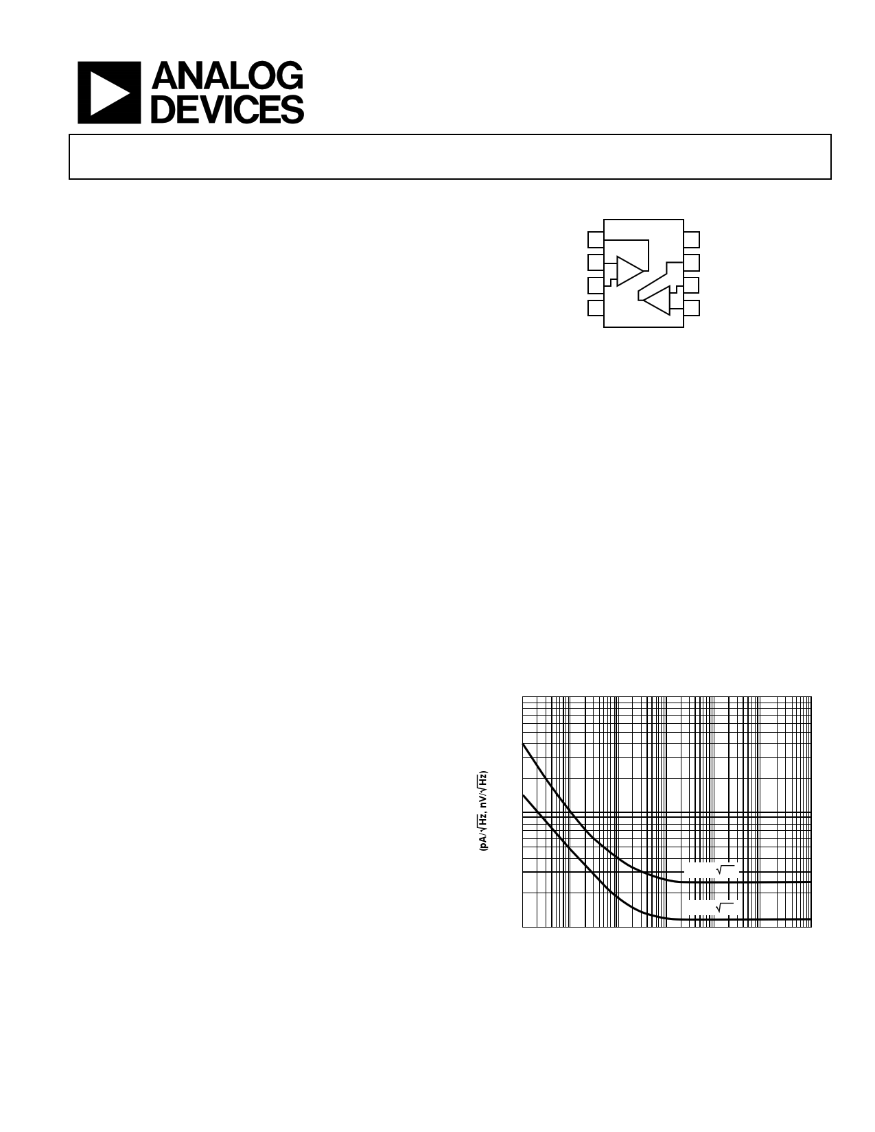
FUNCTIONAL BLOCK DIAGRAM
OUT1 1
–IN1 2
+IN1 3
–VS 4
AD8022
–
+
–
+
8 +VS
7 OUT2
6 –IN2
5 +IN2
Figure 1.
100
10
eN (nV/ Hz)
iN (pA/ Hz)
1
10 100 1k 10k 100k 1M
FREQUENCY (Hz)
Figure 2. Current and Voltage Noise vs. Frequency
10M
One Technology Way, P.O. Box 9106, Norwood, MA 02062-9106, U.S.A.
Tel: 781.329.4700
www.analog.com
Fax: 781.461.3113
©2011 Analog Devices, Inc. All rights reserved.
1 page 
AD8022
Data Sheet
At 25°C, VS = ±2.5 V, RL = 500 Ω, G = +1, TMIN = –40°C, TMAX = +85°C, unless otherwise noted.
Table 2.
Parameter
DYNAMIC PERFORMANCE
−3 dB Small Signal Bandwidth
Bandwidth for 0.1 dB Flatness
Large Signal Bandwidth1
Slew Rate
Rise and Fall Time
Settling Time 0.1%
Overdrive Recovery Time
NOISE/DISTORTION PERFORMANCE
Distortion
Second Harmonic
Third Harmonic
Multitone Input Power Ratio2
Voltage Noise (RTI)
Input Current Noise
DC PERFORMANCE
Input Offset Voltage
Input Offset Current
Input Bias Current
Open-Loop Gain
INPUT CHARACTERISTICS
Input Resistance (Differential)
Input Capacitance
Input Common-Mode Voltage Range
Common-Mode Rejection Ratio
OUTPUT CHARACTERISTICS
Output Voltage Swing
Linear Output Current
Short-Circuit Output Current
Capacitive Load Drive
POWER SUPPLY
Operating Range
Quiescent Current
Power Supply Rejection Ratio
OPERATING TEMPERATURE RANGE
Conditions
VOUT = 50 mV p-p
VOUT = 50 mV p-p
VOUT = 3 V p-p
VOUT = 2 V p-p, G = +2
VOUT = 2 V p-p, G = +2
VOUT = 2 V p-p
VOUT = 150% of max output
voltage, G = +2
VOUT = 2 V p-p
fC = 1 MHz
fC = 1 MHz
G = +7 differential, VS = ±6 V
26 kHz to 132 kHz
144 kHz to 1.1 MHz
f = 100 kHz
f = 100 kHz
TMIN to TMAX
TMIN to TMAX
VCM = ±2.5 V, VS = ±5.0 V
RL = 500 Ω
G = +1, RL = 100 Ω, dc error = 1%
RS = 0 Ω, <3 dB of peaking
TMIN to TMAX
∆VS = ±1 V
Min Typ
100 120
22
4
30 42
40
75
225
−77.5
−94
−69
−66.7
2.3
1
−0.8
±65
2.0
64
20
0.7
−1.83 to +2.0
98
−1.38 to +1.48
±32
80
75
+4.5
3.5
86
−40
1 FPBW = Slew Rate/(2 π VPEAK).
2 Multitone testing performed with 800 mV rms across a 500 Ω load at Point A and Point B on the circuit of Figure 23.
Max Unit
MHz
MHz
MHz
V/μs
ns
ns
ns
dBc
dBc
dBc
dBc
nV/√Hz
pA/√Hz
±5.0
±6.25
5.0
7.5
mV
mV
nA
μA
μA
dB
kΩ
pF
V
dB
V
mA
mA
pF
±13.0
4.25
4.4
+85
V
mA/Amp
mA/Amp
dB
°C
Rev. C | Page 4 of 16
5 Page 
AD8022
0
–0.5
–1.0
–1.5
SIDE A
SIDE B
SIDE A
SIDE B
–2.0
VS = ±2.5V
VS = +12V
–2.5
–60 –40 –20
0 20 40 60 80 100 120 140
TEMPERATURE (°C)
Figure 28. Voltage Offset vs. Temperature
4.5
4.0
3.5
3.0 VS = ±12V
2.5
VS = ±2.5V
2.0
1.5
1.0
0.5
0
–60 –40 –20
0 20 40 60 80 100 120 140
TEMPERATURE (°C)
Figure 29. Bias Current vs. Temperature
4
3 VIN 1kΩ
1kΩ
2
1kΩ
1kΩ
VOUT
500Ω
1 VS = ±2.5V
0
–1
–2
–3 VS = ±12V
–4
–12.5 –10.0 –7.5 –5.0 –2.5 0
2.5 5.0 7.5 10.0 12.5
VCM (V)
Figure 30. Voltage Offset vs. Input Common-Mode Voltage
–50
1kΩ 1kΩ
–60 1kΩ
56.7Ω
–70
1kΩ
50Ω
Data Sheet
–80
–90
–100
1k
8.5
10k 100k
FREQUENCY Hz)
Figure 31. CMRR vs. Frequency
1M
8.0
VS = ±12V
7.5
7.0
6.5
VS = ±2.5V
6.0
5.5
5.0
–50
0 50 100
TEMPERATURE (°C)
150
Figure 32. Total Supply Current vs. Temperature
0
–10
–20
–30
–PSRR
–40
–50
+PSRR
–60
–70
–80
–90
–100
10k
100k
1M
FREQUENCY (Hz)
10M
100M
Figure 33. Power Supply Rejection vs. Frequency VS = ±12 V
Rev. C | Page 10 of 16
11 Page | ||
| Páginas | Total 17 Páginas | |
| PDF Descargar | [ Datasheet AD8022.PDF ] | |
Hoja de datos destacado
| Número de pieza | Descripción | Fabricantes |
| AD802 | Clock Recovery and Data Retiming Phase-Locked Loop | Analog Devices |
| AD8021 | High Speed Amplifier | Analog Devices |
| AD8022 | Low Noise Op Amp | Analog Devices |
| AD8023 | High Current Output/ Triple Video Amplifier | Analog Devices |
| Número de pieza | Descripción | Fabricantes |
| SLA6805M | High Voltage 3 phase Motor Driver IC. |
Sanken |
| SDC1742 | 12- and 14-Bit Hybrid Synchro / Resolver-to-Digital Converters. |
Analog Devices |
|
DataSheet.es es una pagina web que funciona como un repositorio de manuales o hoja de datos de muchos de los productos más populares, |
| DataSheet.es | 2020 | Privacy Policy | Contacto | Buscar |