|
|
|
PDF AD7228 Data sheet ( Hoja de datos )
| Número de pieza | AD7228 | |
| Descripción | LC2MOS Octal 8-Bit DAC | |
| Fabricantes | Analog Devices | |
| Logotipo | ||
Hay una vista previa y un enlace de descarga de AD7228 (archivo pdf) en la parte inferior de esta página. Total 16 Páginas | ||
|
No Preview Available !
Data Sheet
FEATURES
Eight 8-bit DACs with output amplifiers
Operates with single or dual supplies
Microprocessor-compatible (95 ns WR pulse)
No user trims required
Skinny 24-lead PDIP, CERDIP, and SOIC packages, and a
28-lead PLCC surface-mount package
GENERAL DESCRIPTION
The AD7228 contains eight 8-bit voltage mode digital-to- analog
converters (DACs), with output buffer amplifiers and interface
logic on a single monolithic chip. No external trims are required
to achieve the full specified performance for the device.
Separate on-chip latches are provided for each of the eight DACs.
Data is transferred into the data latches through a common
8-bit, TTL/CMOS-compatible input port (5 V). The A0, A1,
and A2 address inputs determine which latch is loaded when
WR goes low. The control logic is speed compatible with most
8-bit microprocessors.
Specified performance is guaranteed for input reference voltages
from 2 V to 10 V when using dual supplies. The device is also
specified for single-supply operation using a reference of 10 V.
Each output buffer amplifier is capable of developing 10 V across a
2 kΩ load.
The AD7228 is fabricated on an all ion implanted, high speed,
linear-compatible CMOS (LC2MOS) process, specifically
Rev. C
Document Feedback
Information furnished by Analog Devices is believed to be accurate and reliable. However, no
responsibility is assumed by Analog Devices for its use, nor for any infringements of patents or other
rights of third parties that may result from its use. Specifications subject to change without notice. No
license is granted by implication or otherwise under any patent or patent rights of Analog Devices.
Trademarksandregisteredtrademarksarethepropertyoftheirrespectiveowners.
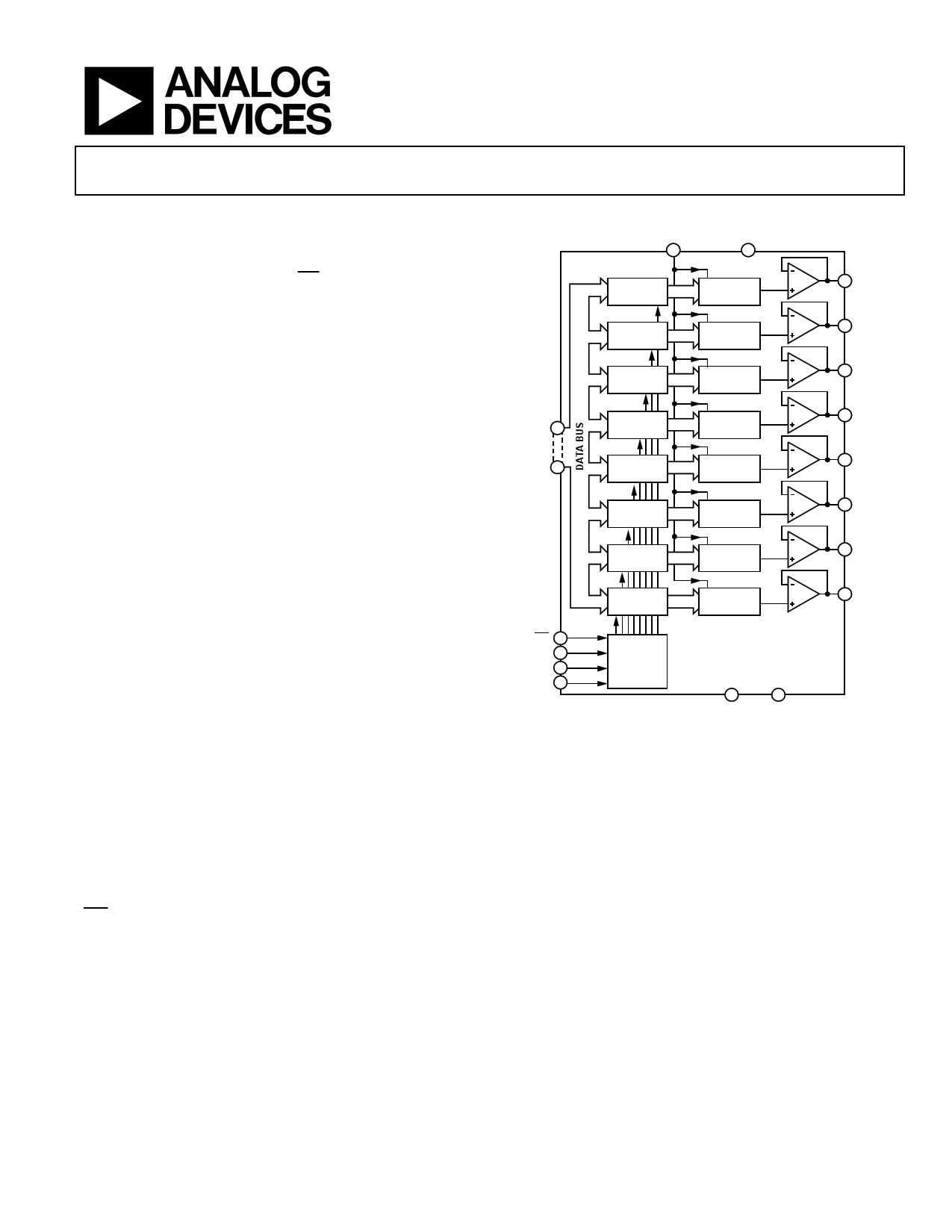
LC2MOS Octal 8-Bit DAC
AD7228
FUNCTIONAL BLOCK DIAGRAM
VREF
VDD
11 1
LATCH 1
DAC 1
1 9 VOUT1
LATCH 2
DAC 2
2 8 VOUT2
LATCH 3
DAC 3
3 7 VOUT3
MSB 13
DATA
(8-BIT)
LSB 20
LATCH 4
LATCH 5
DAC 4
DAC 5
4 6 VOUT4
5 5 VOUT5
LATCH 6
DAC 6
6 4 VOUT6
LATCH 7
DAC 7
7 3 VOUT7
LATCH 8
DAC 8
8 2 VOUT8
WR 21
A2 22
A1 23
A0 24
CONTROL
LOGIC
AD7228
10
VSS
Figure 1.
12
GND
developed to integrate high speed digital logic circuits and
precision analog circuits on the same chip.
PRODUCT HIGHLIGHTS
1. The single chip design of eight 8-bit DACs and amplifiers
allows a dramatic reduction in board space requirements
and offers increased reliability in systems using multiple
converters. The PDIP, CERDIP, and SOIC pinout is aimed at
optimizing board layout with all analog inputs and outputs at
one side of the package and all digital inputs at the other.
2. The voltage mode configuration of the DACs allows single
supply operation of the AD7228. The device can also be
operated with dual supplies giving enhanced performance
for some parameters.
3. The AD7228 has a common 8-bit data bus with individual
DAC latches, providing a versatile control architecture for
simple interface to microprocessors. All latch enable signals
are level triggered and speed compatible with most high
performance 8-bit microprocessors.
One Technology Way, P.O. Box 9106, Norwood, MA 02062-9106, U.S.A.
Tel: 781.329.4700 ©1992–2015 Analog Devices, Inc. All rights reserved.
Technical Support
www.analog.com
1 page 
AD7228
Data Sheet
SINGLE SUPPLY
VDD = 15 V ± 10%, VSS = GND, GND = 0 V, VREF = 10 V, RL = 2 kΩ, CL = 100 pF, unless otherwise noted. All specifications TMIN to TMAX,
−40°C to +85°C, unless otherwise noted.
Table 2.
Parameter
STATIC PERFORMANCE
Resolution
Total Unadjusted Error1
Differential Nonlinearity
Minimum Load Resistance
REFERENCE INPUT
Input Resistance
Input Capacitance2
DIGITAL INPUTS
Input High Voltage, VINH
Input Low Voltage, VINL
Input Leakage Current
Input Capacitance2
Input Coding
DYNAMIC PERFORMANCE2
Voltage Output Slew Rate
Voltage Output Settling Time
Positive Full-Scale Change
Negative Full-Scale Change
Digital Feedthrough
Digital Crosstalk3
POWER SUPPLIES
VDD Range
IDD
at 25°C
TMIN to TMAX
K and B L and C
Versions Versions Unit
Test Conditions/Comments
8 8 Bits
±2 ±1 LSB max
±1
±1
LSB max
Guaranteed monotonic
2
2
kΩ min
VOUT = 10 V
2 2 kΩ min
500 500 pF max Occurs when each DAC is loaded with all 1s
2.4
0.8
±1
8
Binary
2.4
0.8
±1
8
Binary
V min
V max
μA max
pF max
VIN = 0 V or VDD
2 2 V/μs min
5
5
μs max
Settling time to ±1/2 LSB
7
7
μs max
Settling time to ±1/2 LSB
50
50
nV-sec typ
Code transition all 0s to all 1s, VREF = 0 V, WR = VDD
50
50
nV-sec typ
Code transition all 0s to all 1s, VREF = 10 V, WR = 0 V
13.5/16.5
16
20
13.5/16.5
16
20
V min/V max
mA max
mA max
For specified performance
Outputs unloaded; VIN = VINL or VINH
1 Total unadjusted error includes zero code error, relative accuracy and full-scale error.
2 Sample tested at TA = 25°C to ensure compliance.
3 The glitch impulse transferred to the output of one converter (not addressed) due to a change in the digital input code to another addressed converter.
Rev. C | Page 4 of 15
5 Page 
AD7228
Data Sheet
Table 7. Unipolar Code Table
DAC Latch Contents
MSB
LSB1
Analog Output
1111
1000
1000
1111
0001
0000
+VREF(255/256)
+VREF(129/256)
+VREF 128 VREF
256 2
0111
0000
0000
1111
0001
0000
+VREF(127/256)
+VREF(1/256)
0V
1 1 LSB = (VREF)(2−8) = VREF (1/256).
Bipolar Output Operation
Each of the DACs on the AD7228 can be individually configured
for bipolar output operation. This is possible using one external
amplifier and two resistors per channel. Figure 11 shows a circuit
used to implement offset binary coding (bipolar operation) with
DAC 1 of the AD7228. In this case,
VOUT
1
R2
R1
(D1
VREF )
R2
R1
(VREF
)
With R1 = R2,
VOUT = (2D1 − 1) × (VREF)
where D1 is a fractional representation of the digital word in
Latch 1 of the AD7228 (0 ≤ D1 ≤ 255/256).
VREF
VREF
11
VDD
1
Table 8. Bipolar Code Table
DAC Latch Contents
MSB LSB
1111
1111
1000
0001
1000
0000
0111
1111
0000
0001
0000
0000
Analog Output
+VREF(127/128)
+VREF(1/128)
0V
−VREF(1/128)
−VREF(127/128)
−VREF(128/128) = −VREF
Mismatch between R1 and R2 causes gain and offset errors;
therefore, these resistors must match and track over temperature.
The AD7228 can be operated from a single supply or from dual
supplies. Table 8 shows the digital code vs. output voltage
relationship for the circuit of Figure 11 with R1 = R2.
AC Reference Signal
In some applications, it may be desirable to have an ac signal
applied as the reference input to the AD7228. The AD7228 has
multiplying capability within the upper (10 V) and lower (2 V)
limits of reference voltage when operated with dual supplies.
Therefore, ac signals must be ac-coupled and biased up before
being applied to the reference input. Figure 12 shows an ac
signal applied to the reference input of the AD7228. For input
frequencies up to 50 kHz, the output distortion typically remains
less than 0.1%. The typical 3 dB bandwidth for small signal
inputs is 800 kHz.
R1
10kΩ
±0.1%
R2
10kΩ
±0.1%
+15V
DAC 1
9 VOUT1
AD7228*
–15V
VOUT
10
VSS
12
GND
*ADDITIONAL PINS OMITTED FOR CLARITY.
Figure 11. Bipolar Output Circuit
+4V
REFERENCE
INPUT
–4V
+15V
15kΩ
10kΩ
+10V
+2V
VREF
11
+15V
VDD
1
DAC 1
9 VOUT1
AD7228*
*ADDITIONAL PINS OMITTED FOR CLARITY.
10
VSS
–5V
12
GND
Figure 12. Applying an AC Signal to the AD7228
Rev. C | Page 10 of 15
11 Page | ||
| Páginas | Total 16 Páginas | |
| PDF Descargar | [ Datasheet AD7228.PDF ] | |
Hoja de datos destacado
| Número de pieza | Descripción | Fabricantes |
| AD722 | RGB to NTSC/PAL Encoder | Analog Devices |
| AD7224 | LC2MOS 8-Bit DAC with Output Amplifiers | Analog Devices |
| AD7225 | LC2MOS Quad 8-Bit DAC with Separate Reference Inputs | Analog Devices |
| AD7226 | LC2MOS Quad 8-Bit D/A Converter | Analog Devices |
| Número de pieza | Descripción | Fabricantes |
| SLA6805M | High Voltage 3 phase Motor Driver IC. |
Sanken |
| SDC1742 | 12- and 14-Bit Hybrid Synchro / Resolver-to-Digital Converters. |
Analog Devices |
|
DataSheet.es es una pagina web que funciona como un repositorio de manuales o hoja de datos de muchos de los productos más populares, |
| DataSheet.es | 2020 | Privacy Policy | Contacto | Buscar |