|
|
|
PDF BD37067FV-M Data sheet ( Hoja de datos )
| Número de pieza | BD37067FV-M | |
| Descripción | Sound Processor | |
| Fabricantes | ROHM Semiconductor | |
| Logotipo | ||
Hay una vista previa y un enlace de descarga de BD37067FV-M (archivo pdf) en la parte inferior de esta página. Total 30 Páginas | ||
|
No Preview Available !
Datasheet
Analog Sound Processors series
Sound Processor for car audio
built-in 2nd order post filter
BD37067FV-M
General Description
It is built-in input selector of 6 stereo source and output
to ADC after adjusting signal level. And built-in 2nd order
post filter to reduce out of band noise and 6ch Volume
circuit. Moreover, it is simple to design set by built-in
TDMA noise reduction systems.
Features
AEC-Q100 (Grade3) Qualified
Built-in differential input selector that can select
single-ended / differential input
Reduce the pop noise when switching gain due to
built-in advanced switch circuit
Less out-of-band noise of DAC by built-in 2nd order
post filter.
Built-in buffered ground isolation amplifier to realize
high CMRR characteristics
Built-in TDMA noise reduction circuit reduces the
additional components for external filter.
Package is SSOP-B40. Putting same direction
input-terminals and output-terminals make PCB
layout easier and PCB area smaller.
Available to control by 3.3V / 5V for I2C-bus
controller.
Key Specifications
Total Harmonic Distortion:
0.003%(Typ)
Maximum Input Voltage:
2.2VRMS(Typ)
Common Mode Rejection Ratio:
55dB(Min)
Maximum Output Voltage:
2.1VRMS(Typ)
Output Noise Voltage:
8μVRMS(Typ)
Residual Output Noise Voltage:
Ripple Rejection:
2.5μVRMS(Typ)
-70dB (Typ)
Operating Temperature Range: -40 ˚C to +85˚C
Package
SSOP-B40
W(Typ) x D(Typ) x H(Max)
13.60mm x 7.80mm x 2.00mm
Applications
It is the optimal for the car audio. Besides, it is
possible to use for the audio equipment of mini
Compo, micro Compo.
SSOP-B40
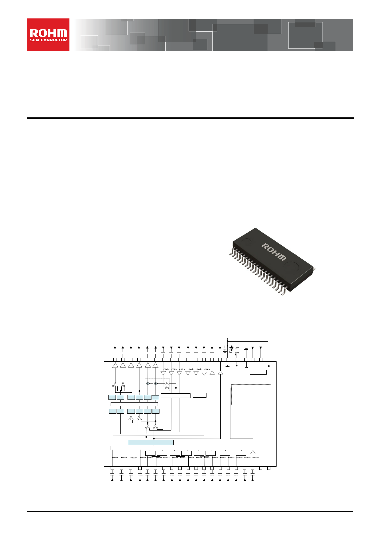
Typical Application Circuit
VCC
OUTC OUTS OUTR1 OUTR2 OUTF1 OUTF2 INF2 INF1 INR2 INR1 INS INC IG1 IG210µF 10µF
GND SDA SCL
10µF 10µF 10µF 10µF 10µF 10µF 2.2µF 2.2µF 2.2µF 2.2µF 2.2µF 2.2µF 10µF
10µF
40 39 38 37 36 35 34 33 32 31 30 29 28 27
10µF
VCC1 VREF
26 25 24
23
22
VCC2
21
Sub
Selector
100kΩ 100kΩ 100kΩ 100kΩ 100kΩ 100kΩ
Front Mixing
★★
Fader
ATT★
Fader
ATT★
Fader
ATT★
Fader
ATT★
Fader
ATT★
Fader
ATT★
2nd order LPF
Fader
Boost★
Fader
Boost★
Fader
Boost★
Fader
Boost★
Fader
Boost★
Fader
Boost★
Rear
Selector
Front
Selector
Main Gain Adjust
Sub
Gain Adjust
VREF
I2C-bus LOGIC
■Fader : +23dB to -79dB、-∞/1dBstep
■Input Gain : +23dB to -15dB/1dBstep
■Front Mixing : on/off
★ Advanced Switch
■2nd order LPF: fc=70kHz
■Main/Sub Gain Adjust 0dB/6dB
■Anti-TDMA noise circuit
★ Input Gain
100kΩ
100kΩ
250kΩ
GND
ISO amp
Input selector (2 single - end and 4 stereo ISO)
GND
ISO amp
GND
ISO amp
GND
ISO amp
GND
ISO amp
GND
ISO amp
Differential
amp
Differential
amp
250kΩ 250kΩ 250kΩ 250kΩ 250kΩ 250kΩ 250kΩ 250kΩ 250kΩ 250kΩ 250kΩ 250kΩ 250kΩ 250kΩ 100kΩ
1 2 3 4 5 6 7 8 9 10 11 12 13 14 15 16 17 18 19 20
TEST1 TEST2
2.2µF 2.2µF 2.2µF 2.2µF 2.2µF 10µF 2.2µF 2.2µF 10µF 2.2µF 2.2µF 10µF 2.2µF 2.2µF 10µF 10µF 2.2µF 2.2µF
A1 A2 B1
B2 CP1 CN CP2 DP1 DN
DP2 EP1
EN EP2 FP1 FN1 FN2 FP2 MIN
Figure 1. Typical Application Circuit
○Product structure:Silicon monolithic integrated circuit
www.rohm.com
© 2014 ROHM Co., Ltd. All rights reserved.
TSZ22111・14・001
○This product is not designed protection against radioactive rays.
1/34
TSZ02201-0C2C0E100140-1-2
14.NOV.2016 Rev.002
1 page 
BD37067FV-M
Electrical Characteristic
(Unless specified particularly, Ta=25˚C, VCC1,2=8.5V, f=1kHz, VIN=1VRMS, RG=600Ω, RL=10kΩ,
A input, Input Gain 0dB, Gain Adjust +6dB, LPF ON, Fader 0dB, Input point=A1/A2, Monitor point=IG1/IG2)
Parameter
Limit
Symbol Min Typ Max
Unit
Conditions
Current upon no signal
(IQ_VCC1+IQ_VCC2)
IQ_VCC - 35 53 mA No signal
Input Impedance (A)
RIN_S
70 100 130
kΩ
Input Impedance (B, C, D, E, F)
RIN_D
175 250 325
kΩ
Voltage Gain
GV
-1.5 +0 +1.5
dB Gv=20log(VOUT/VIN)
Channel Balance
Total Harmonic Distortion
Output Noise Voltage(Note1)
Maximum Input Voltage
Crosstalk Between Channels(Note1)
Crosstalk Between Selectors(Note1)
Common Mode Rejection Ratio
(C, D, E, F) (Note1)
CB
THD+N
VNO1
VIM
CTC
CTS
CMRR
-1.5 +0 +1.5
- 0.003 0.05
- 3.1 8.0
2.0 2.2 -
- -100 -90
- -100 -90
55 65 -
dB
%
μVRMS
VRMS
dB
dB
dB
CB = GV1-GV2
VOUT =1VRMS
BW=400-30kHz
RG = 0Ω
BW = IHF-A
VIM at THD+N(VOUT)=1%
BW=400-30kHz
RG = 0Ω
CTC=20log(VOUT/VOUT´)
BW = IHF-A
RG = 0Ω
CTS=20log(VOUT/VOUT´)
BW = IHF-A
XP1 and XN input
XP2 and XN input
CMRR=20log(VIN/VOUT)
BW = IHF-A, [X=C,D,E,F]
Minimum Input Gain
Maximum Input Gain
Gain Set Error
GIN MIN -17 -15 -13
GIN MAX
21
23
25
GIN ERR
-2
+0
+2
dB
Input gain -15dB
Gin=20log(VOUT/VIN)
Input gain 23dB
dB VIN =100mVRMS
Gin=20log(VOUT/VIN)
dB GAIN=-15 to +23dB
Output Impedance
ROUT
- - 50
Ω VIN =100mVRMS
Maximum Output Voltage
VOM
2.0 2.2
-
VRMS
THD+N=1%
BW=400-30kHz
(Note1) VP-9690A (Average value detection, effective value display) filter by Panasonic is used for measurement. Input and output are in-phase.
(Unless specified particularly, Ta=25˚C, VCC1,2=8.5V, f=1kHz, VIN=0.9VRMS, RG=600Ω, RL =10kΩ,
A input, Input Gain 0dB, Gain Adjust +6dB, LPF ON, Fader 0dB,
Input point=INF1/INF2/INR1/INR2/INC/INS, Monitor point=OUTF1/OUTF2/OUTR1/OUTR2/OUTC/OUTS)
Parameter
Symbol Min
Limit
Typ
Max
Unit
Conditions
Output Impedance
Maximum Output Voltage
ROUT
-
- 50
Ω VIN =100mVRMS
VOM
2.0 2.1
-
VRMS
THD+N=1%
BW=400-30kHz
www.rohm.com
© 2014 ROHM Co., Ltd. All rights reserved.
TSZ22111・15・001
5/34
TSZ02201-0C2C0E100140-1-2
14.NOV.2016 Rev.002
5 Page 
BD37067FV-M
5. Select Address & Data
Items
Initial Setup 1
Select
Address
(hex)
01
MSB
D7
Advanced
Switch
ON/OFF
Initial Setup 2
02 0
D6
0
0
Input Selector
Input Gain
Fader 1ch Front
Fader 2ch Front
Fader 1ch Rear
Fader 2ch Rear
Fader Center
Fader Subwoofer
LPF setup
Mixing
System Reset
05 0
0
06 0
0
28
29
2A
2B
2C
2D
Front
30 Mixing LPF fc
ON/OFF
FE 1
0
Data
D5 D4 D3
Advanced Switch
time of Input
Gain/Fader
0
Sub Selector
0
LSB
D2 D1 D0
0 00
0
Rear
Front
Selector Selector
00
Input Selector
Input Gain
Fader Gain / Attenuation
Fader Gain / Attenuation
Fader Gain / Attenuation
Fader Gain / Attenuation
Fader Gain / Attenuation
Fader Gain / Attenuation
000
0
00 0
0
Sub
Gain
Adjust
0
Main
Gain
Adjust
1
Advanced switch
Note) Set up bit (It is written with “0” by the above table) which hasn’t been used in “0”.
Notes on data format
1. “Advanced switch” function is available for the hatched parts on the above table.
2. In case of transferring data continuously, Select Address(hex) flows by Automatic increment function, as shown
below.
→01→02→05→06→28→29→2A→2B→2C→2D→30
3. Input selector that is not corresponded for “Advanced switch” function, cannot reduce the noise caused when
changing the input selector. Therefore, it is recommended to turn on mute when changing these settings.
4. In case of setting to infinite “-∞” by using Fader when input selector setting is changed, please consider “Advanced
switch” time.
www.rohm.com
© 2014 ROHM Co., Ltd. All rights reserved.
TSZ22111・15・001
11/34
TSZ02201-0C2C0E100140-1-2
14.NOV.2016 Rev.002
11 Page | ||
| Páginas | Total 30 Páginas | |
| PDF Descargar | [ Datasheet BD37067FV-M.PDF ] | |
Hoja de datos destacado
| Número de pieza | Descripción | Fabricantes |
| BD37067FV-M | Sound Processor | ROHM Semiconductor |
| Número de pieza | Descripción | Fabricantes |
| SLA6805M | High Voltage 3 phase Motor Driver IC. |
Sanken |
| SDC1742 | 12- and 14-Bit Hybrid Synchro / Resolver-to-Digital Converters. |
Analog Devices |
|
DataSheet.es es una pagina web que funciona como un repositorio de manuales o hoja de datos de muchos de los productos más populares, |
| DataSheet.es | 2020 | Privacy Policy | Contacto | Buscar |