|
|
|
PDF BD3464FV Data sheet ( Hoja de datos )
| Número de pieza | BD3464FV | |
| Descripción | General-Purpose 4ch Electronic Volume | |
| Fabricantes | ROHM Semiconductor | |
| Logotipo | ||
Hay una vista previa y un enlace de descarga de BD3464FV (archivo pdf) en la parte inferior de esta página. Total 30 Páginas | ||
|
No Preview Available !
Datasheet
General-Purpose 4ch Electronic Volume
with Built-in Advanced Switch
BD3464FV
General Description
BD3464FV is a 4ch electronic volume which has the
best audio efficiency in the industry. It has a volume
switching shock sound prevention technique called
“Advanced Switch,” supporting the construction of high
quality car audio space by simple control.
Features
Reduce switching noise of volume by using
Advanced Switch circuit.
Energy-saving design resulting in low-current
consumption by utilizing the Bi-CMOS process. It
has the advantage in quality over scaling down the
power heat control of the internal regulators.
Arranges all I/O terminals together for easier PCB
layout and smaller PCB area.
I2C BUS can be controlled by 3.3V / 5V.
Key Specifications
Power Supply Voltage Range:
Circuit Current (no signal):
Total Harmonic Distortion:
Maximum Input Voltage:
Cross-talk between Selectors:
Volume Control Range:
Output Noise Voltage:
Residual Output Noise Voltage:
Operating Temperature Range:
7.0V to 9.5V
25mA (Typ)
0.0004%(Typ)
2.35Vrms (Typ)
-105dB (Typ)
+23dB to -79dB
1.9µVrms(Typ)
1.6µVrms (Typ)
-40°C to +85°C
Package
W(Typ) x D(Typ) x H(Max)
Applications
It is optimal for car audio. It can also be used for car
navigation, audio equipment of mini Compo, micro
Compo, DVD, TV, etc.
SSOP-B20
6.50mm x 6.40mm x 1.45mm
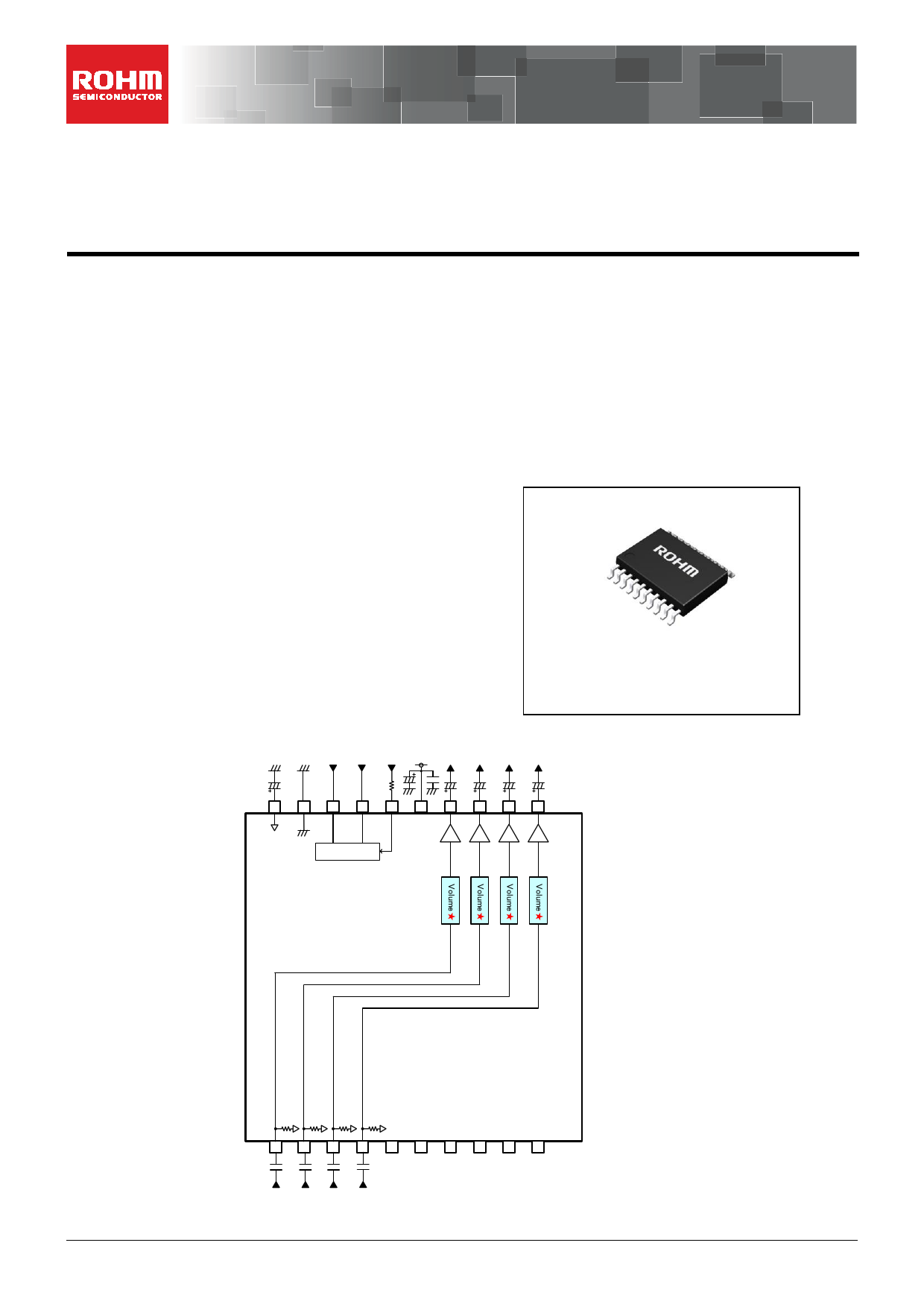
Typical Application Circuit
FIL GND
10μ
SDA
SCL CS VCC OUTF1 OUTF2 OUTR1 OUTR2
10μ
0.1μ
4.7μ
4.7μ
4.7μ
4.7μ
2.2K
20 19 18 17 16 15 14 13 12 11
VCC
VCC/2 GND
I2C BUS LOGIC
■4 ch Volume
++2233ddBB~to --7799ddBB/1/d1BdBstespt,e-p∞,- ∞
★: Advanced switch circuit
100k 100k 100k 100k
1 2 3 4 5 6 7 8 9 10
1μ 1μ 1μ 1μ
INF1 INF2 INR1 INR2
Unit
R : [Ω]
C : [F]
○Product structure:Silicon monolithic integrated circuit
www.rohm.com
© 2015 ROHM Co., Ltd. All rights reserved.
TSZ22111・14・001
○This product has no designed protection against radioactive rays
1/26
TSZ02201-0C2C0E100370-1-2
16.Dec.2015 rev.001
1 page 
BD3464FV
Electrical Characteristics – continued
(Unless specified, Ta=25°C, VCC=8.5V, f=1kHz, VIN=1Vrms, Rg=600Ω, RL=10kΩ, INF1 input, Volume 0dB)
Limit
Parameter
Symbol
Unit
Min Typ Max
Conditions
Input Impedance
RIN_V
70 100 130 kΩ
Maximum Input Voltage
VIM
2 2.35 - Vrms VIM AT THD+N(VOUT)=1%
BW=400Hz-30KHz
Maximum Gain
Maximum Attenuation *
GV_BST
GV_MIN
21 23 25
- -109 -90
GAIN=23DB
dB VIN=100mVrms
GV=20log(VOUT/VIN)
Volume=-∞dB
dB GV=20log(VOUT/VIN)
BW=IHF-A
Step Resolution
GV_STEP
-
1
- dB GAIN&ATT=+23dB to -79dB
Gain Set Error
GV_ERR
-2
0
+2 dB GAIN=+1dB to +23dB
Attenuation Set Error 1
GV_ERR1
-2
0
+2 dB ATT=-1dB to -15dB
Attenuation Set Error 2
GV_ERR2
-3
0
+3 dB ATT=-16dB to -47dB
Attenuation Set Error 3
Output Impedance
GV_ERR3
ROUT
-4
-
0 +4 dB ATT=-48dB to -79dB
- 50
Ω VIN =100mVrms
Maximum Output Voltage
VOM
2 2.35 - Vrms THD+N=1%
BW=400Hz-30kHz
VP-9690A (Average value detection, effective value display) filter by Matsushita Communication is used for * measurement.
Phase between input / output is same.
www.rohm.com
© 2015 ROHM Co., Ltd. All rights reserved.
TSZ22111・15・001
5/26
TSZ02201-0C2C0E100370-1-2
16.Dec.2015 rev.001
5 Page 
BD3464FV
(2) I2C BUS FORMAT
MSB
LSB
S Slave Address
1bit 8bit
S
Slave Address
A
Select Address
Data
P
MSB
LSB MSB
LSB
A Select Address A
Data
AP
1bit 8bit 1bit 8bit 1bit 1bit
= Start condition (Recognition of start bit)
= Recognition of slave address. The first 7 bits correspond to the slave address.
The least significant bit is “L” which corresponds to write mode.
= ACKNOWLEDGE bit (Recognition of acknowledgement)
= Select address corresponding to volume, bass or treble.
= Data on every volume and tone.
= Stop condition (Recognition of stop bit)
(3) I2C BUS Interface Protocol
(a) Basic format
S Slave Address
MSB
LSB
A Select Address
MSB
LSB
A Data A P
MSB LSB
(b) Automatic increment (Select Address increases (+1) according to the number of data.
S Slave Address A Select Address A Data1 A Data2 A ・・・・
MSB
(Example)
LSB MSB
LSB MSB LSB
MSB LSB
①Data1 shall be set as data of address specified by Select Address.
②Data2 shall be set as data of address specified by Select Address +1.
③DataN shall be set as data of address specified by Select Address +N-1.
DataN
MSB
AP
LSB
(c) Configuration unavailable for transmission (In this case, only Select Address1 is set.
S Slave Address A Select Address1 A Data A Select Address 2 A Data A
MSB
LSB MSB
LSB MSB LSB MSB
LSB MSB LSB
(Note)If any data is transmitted as Select Address 2 next to data, it is recognized
as data, not as Select Address 2.
P
(4) Slave Address
Because the slave address can be changed by the setting of CS, it is possible to use two chips at the same time
on identical BUS.
MSB
LSB
SEL Voltage Condition
GND to 0.2 x VCC
0.8 x VCC to VCC
A6 A5 A4 A3 A2 A1 A0 R/W
1 0 0 0 0 0 0 0 80H
84H
10000100
Establish the CS voltage to define the setting.
www.rohm.com
© 2015 ROHM Co., Ltd. All rights reserved.
TSZ22111・15・001
11/26
TSZ02201-0C2C0E100370-1-2
16.Dec.2015 rev.001
11 Page | ||
| Páginas | Total 30 Páginas | |
| PDF Descargar | [ Datasheet BD3464FV.PDF ] | |
Hoja de datos destacado
| Número de pieza | Descripción | Fabricantes |
| BD3464FV | General-Purpose 4ch Electronic Volume | ROHM Semiconductor |
| Número de pieza | Descripción | Fabricantes |
| SLA6805M | High Voltage 3 phase Motor Driver IC. |
Sanken |
| SDC1742 | 12- and 14-Bit Hybrid Synchro / Resolver-to-Digital Converters. |
Analog Devices |
|
DataSheet.es es una pagina web que funciona como un repositorio de manuales o hoja de datos de muchos de los productos más populares, |
| DataSheet.es | 2020 | Privacy Policy | Contacto | Buscar |