|
|
|
PDF ADV7123 Data sheet ( Hoja de datos )
| Número de pieza | ADV7123 | |
| Descripción | Triple 10-Bit High Speed Video DAC | |
| Fabricantes | Analog Devices | |
| Logotipo | ||
Hay una vista previa y un enlace de descarga de ADV7123 (archivo pdf) en la parte inferior de esta página. Total 25 Páginas | ||
|
No Preview Available !
CMOS, 330 MHz
Triple 10-Bit High Speed Video DAC
ADV7123
FEATURES
330 MSPS throughput rate
Triple 10-bit digital-to-analog converters (DACs)
SFDR
−70 dB at fCLK = 50 MHz; fOUT = 1 MHz
−53 dB at fCLK = 140 MHz; fOUT = 40 MHz
RS-343A-/RS-170-compatible output
Complementary outputs
DAC output current range: 2.0 mA to 26.5 mA
TTL-compatible inputs
Internal reference (1.235 V)
Single-supply 5 V/3.3 V operation
48-lead LQFP package
Low power dissipation (30 mW minimum @ 3 V)
Low power standby mode (6 mW typical @ 3 V)
Industrial temperature range (−40°C to +85°C)
Pb-free (lead-free) package
APPLICATIONS
Digital video systems (1600 × 1200 @ 100 Hz)
High resolution color graphics
Digital radio modulation
Image processing
Instrumentation
Video signal reconstruction
GENERAL DESCRIPTION
The ADV7123 (ADV®) is a triple high speed, digital-to-analog
converter on a single monolithic chip. It consists of three high
speed, 10-bit, video DACs with complementary outputs, a
standard TTL input interface, and a high impedance, analog
output current source.
The ADV7123 has three separate 10-bit-wide input ports. A
single 5 V/3.3 V power supply and clock are all that are required
to make the part functional. The ADV7123 has additional video
control signals, composite SYNC and BLANK.
The ADV7123 also has a power save mode.
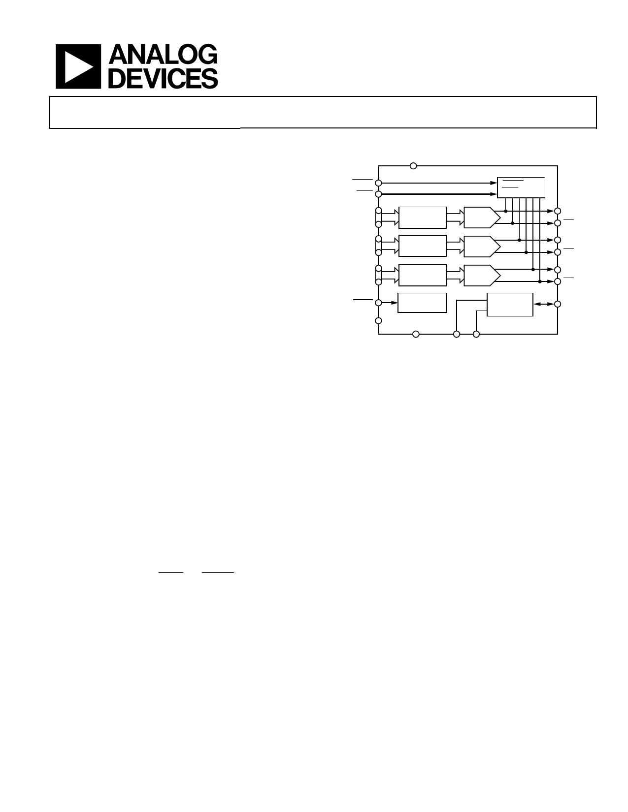
FUNCTIONAL BLOCK DIAGRAM
VAA
BLANK
SYNC
BLANK AND
SYNC LOGIC
R9 TO R0 10
DATA
REGISTER
10
DAC
G9 TO G0 10
DATA
REGISTER
10
DAC
B9 TO B0 10
DATA
REGISTER
10
DAC
PSAVE
CLOCK
POWER-DOWN
MODE
VOLTAGE
REFERENCE
CIRCUIT
ADV7123
GND
RSET COMP
Figure 1.
IOR
IOR
IOG
IOG
IOB
IOB
VREF
The ADV7123 is fabricated in a 5 V CMOS process. Its
monolithic CMOS construction ensures greater functionality
with lower power dissipation. The ADV7123 is available in a
48-lead LQFP package.
PRODUCT HIGHLIGHTS
1. 330 MSPS throughput.
2. Guaranteed monotonic to 10 bits.
3. Compatible with a wide variety of high resolution color
graphics systems, including RS-343A and RS-170.
ADV is a registered trademark of Analog Devices, Inc.
Rev. D
Information furnished by Analog Devices is believed to be accurate and reliable. However, no
responsibility is assumed by Analog Devices for its use, nor for any infringements of patents or other
rights of third parties that may result from its use. Specifications subject to change without notice. No
license is granted by implication or otherwise under any patent or patent rights of Analog Devices.
Trademarksandregisteredtrademarksarethepropertyoftheirrespectiveowners.
One Technology Way, P.O. Box 9106, Norwood, MA 02062-9106, U.S.A.
Tel: 781.329.4700
www.analog.com
Fax: 781.461.3113
©2010 Analog Devices, Inc. All rights reserved.
1 page 
ADV7123
3.3 V SPECIFICATIONS
VAA = 3.0 V to 3.6 V, VREF = 1.235 V, RSET = 560 Ω, CL = 10 pF. All specifications TMIN to TMAX,1 unless otherwise noted, TJ MAX = 110°C.
Table 2.
Parameter2
STATIC PERFORMANCE
Resolution (Each DAC)
Integral Nonlinearity (BSL)
Differential Nonlinearity
DIGITAL AND CONTROL INPUTS
Input High Voltage, VIH
Input Low Voltage, VIL
Input Current, IIN
PSAVE Pull-Up Current
Input Capacitance, CIN
ANALOG OUTPUTS
Output Current
DAC-to-DAC Matching
Output Compliance Range, VOC
Output Impedance, ROUT
Output Capacitance, COUT
Offset Error
Gain Error3
VOLTAGE REFERENCE, EXTERNAL
Reference Range, VREF
VOLTAGE REFERENCE, INTERNAL
Voltage Reference, VREF
POWER DISSIPATION
Digital Supply Current4
Analog Supply Current
Standby Supply Current
Power Supply Rejection Ratio
Min Typ
Max Unit
Test Conditions1
10
−1 +0.5 +1
−1 +0.25 +1
2.0
0.8
−1
20
10
+1
Bits
LSB
LSB
V
V
μA
μA
pF
RSET = 680 Ω
RSET = 680 Ω
RSET = 680 Ω
VIN = 0.0 V or VDD
2.0
2.0
1.0
0
70
10
0
0
26.5 mA
Green DAC, SYNC = high
18.5 mA
RGB DAC, SYNC = low
%
1.4 V
kΩ
pF
0 % FSR Tested with DAC output = 0 V
% FSR FSR = 17.62 mA
1.12 1.235 1.35 V
1.235
V
2.2 5.0 mA fCLK = 50 MHz
6.5 12.0 mA fCLK = 140 MHz
11 15 mA fCLK = 240 MHz
16 mA fCLK = 330 MHz
67
72 mA
RSET = 560 Ω
8 mA RSET = 4933 Ω
2.1 5.0 mA PSAVE = low, digital, and control inputs at VDD
0.1 0.5 %/%
1 Temperature range TMIN to TMAX: −40°C to +85°C at 50 MHz and 140 MHz, 0°C to 70°C at 240 MHz and 330 MHz.
2 These maximum/minimum specifications are guaranteed by characterization to be over the 3.0 V to 3.6 V range.
3 Gain error = {(Measured (FSC)/Ideal (FSC) − 1) × 100}, where Ideal = VREF/RSET × K × (0x3FFH) and K = 7.9896.
4 Digital supply is measured with a continuous clock that has data input corresponding to a ramp pattern and with an input level at 0 V and VDD.
Rev. D | Page 4 of 24
5 Page 
ADV7123
PIN CONFIGURATION AND FUNCTION DESCRIPTIONS
48 47 46 45 44 43 42 41 40 39 38 37
G0 1
G1 2
G2 3
G3 4
G4 5
G5 6
G6 7
G7 8
G8 9
G9 10
BLANK 11
SYNC 12
PIN 1
INDICATOR
ADV7123
TOP VIEW
(Not to Scale)
36 VREF
35 COMP
34 IOR
33 IOR
32 IOG
31 IOG
30 VAA
29 VAA
28 IOB
27 IOB
26 GND
25 GND
13 14 15 16 17 18 19 20 21 22 23 24
Figure 3. Pin Configuration
Table 8. Pin Function Descriptions
Pin No. Mnemonic Description
1 to 10,
14 to 23,
39 to 48
G0 to G9,
B0 to B9,
R0 to R9
Red, Green, and Blue Pixel Data Inputs (TTL Compatible). Pixel data is latched on the rising edge of CLOCK. R0,
G0, and B0 are the least significant data bits. Unused pixel data inputs should be connected to either the
regular printed circuit board (PCB) power or ground plane.
11
BLANK
Composite Blank Control Input (TTL Compatible). A Logic 0 on this control input drives the analog outputs,
IOR, IOB, and IOG, to the blanking level. The BLANK signal is latched on the rising edge of CLOCK. While
BLANK is a Logic 0, the R0 to R9, G0 to G9, and B0 to B9 pixel inputs are ignored.
12 SYNC Composite Sync Control Input (TTL Compatible). A Logic 0 on the SYNC input switches off a 40 IRE current
source. This is internally connected to the IOG analog output. SYNC does not override any other control or
data input; therefore, it should only be asserted during the blanking interval. SYNC is latched on the rising
edge of CLOCK. If sync information is not required on the green channel, the SYNC input should be tied to
Logic 0.
13, 29, 30 VAA
24 CLOCK
Analog Power Supply (5 V ± 5%). All VAA pins on the ADV7123 must be connected.
Clock Input (TTL Compatible). The rising edge of CLOCK latches the R0 to R9, G0 to G9, B0 to B9, SYNC, and
BLANK pixel and control inputs. It is typically the pixel clock rate of the video system. CLOCK should be driven
by a dedicated TTL buffer.
25, 26
GND
Ground. All GND pins must be connected.
27, 31, 33
IOB, IOG, IOR
Differential Red, Green, and Blue Current Outputs (High Impedance Current Sources). These RGB video
outputs are specified to directly drive RS-343A and RS-170 video levels into a doubly terminated 75 Ω load. If
the complementary outputs are not required, these outputs should be tied to ground.
28, 32, 34
IOB, IOG, IOR
Red, Green, and Blue Current Outputs. These high impedance current sources are capable of directly driving a
doubly terminated 75 Ω coaxial cable. All three current outputs should have similar output loads whether or
not they are all being used.
35
COMP
Compensation Pin. This is a compensation pin for the internal reference amplifier. A 0.1 μF ceramic capacitor
must be connected between COMP and VAA.
36 VREF
Voltage Reference Input for DACs or Voltage Reference Output (1.235 V).
Rev. D | Page 10 of 24
11 Page | ||
| Páginas | Total 25 Páginas | |
| PDF Descargar | [ Datasheet ADV7123.PDF ] | |
Hoja de datos destacado
| Número de pieza | Descripción | Fabricantes |
| ADV7120 | CMOS 80 MHz/ Triple 8-Bit Video DAC | Analog Devices |
| ADV7121 | CMOS 80 MHz/ Triple 10-Bit Video DACs | Analog Devices |
| ADV7122 | CMOS 80 MHz/ Triple 10-Bit Video DACs | Analog Devices |
| ADV7123 | Triple 10-Bit High Speed Video DAC | Analog Devices |
| Número de pieza | Descripción | Fabricantes |
| SLA6805M | High Voltage 3 phase Motor Driver IC. |
Sanken |
| SDC1742 | 12- and 14-Bit Hybrid Synchro / Resolver-to-Digital Converters. |
Analog Devices |
|
DataSheet.es es una pagina web que funciona como un repositorio de manuales o hoja de datos de muchos de los productos más populares, |
| DataSheet.es | 2020 | Privacy Policy | Contacto | Buscar |