|
|
|
PDF HI-3587 Data sheet ( Hoja de datos )
| Número de pieza | HI-3587 | |
| Descripción | Transmitter | |
| Fabricantes | HOLTIC | |
| Logotipo | ||
Hay una vista previa y un enlace de descarga de HI-3587 (archivo pdf) en la parte inferior de esta página. Total 11 Páginas | ||
|
No Preview Available !
June 2009
HI-3587
ARINC 429
Transmitter with SPI Interface
GENERAL DESCRIPTION
The HI-3587 from Holt Integrated Circuits is a silicon gate
CMOS device for interfacing a Serial Peripheral Interface
(SPI) enabled microcontroller to an ARINC 429 serial bus.
The device provides one ARINC 429 transmitter with 32 X
32 Transmit FIFO and built-in line driver. Transmit FIFO
status can be monitored using the programmable external
interrupt pin, or by polling the HI-3587 Status Register.
Other features include a programmable option of data or
parity in the 32nd bit, and the ability to switch the bit-
signifiance of ARINC 429 labels. Line driver output pins
are available with different values of output resistance to
provide flexibility when using external lightning protection
circuitry.
The Serial Peripheral Interface minimizes the number of
host interface signals and provides a small footprint device
that can be interfaced to a wide variety of industry-
standard microcontrollers supporting SPI. Alternatively,
the SPI signals may be controlled using four general
purpose I/O port pins from a microcontroller or custom
FPGA. The SPI and all control signals are CMOS and TTL
compatible and support 3.3V or 5V operation.
The HI-3587 applies the ARINC 429 protocol to the
transmitter. ARINC 429 databus timing comes from a 1
MHz clock input, or an internal counter can derive it from
higher clock frequencies having certain fixed values,
possibly the external host processor clock.
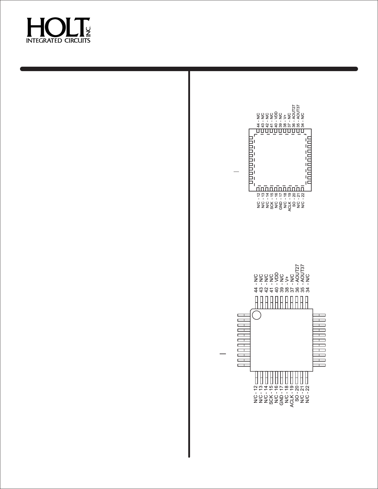
PIN CONFIGURATIONS (Top View)
N/C - 1
N/C - 2
N/C - 3
N/C - 4
N/C - 5
N/C - 6
MR - 7
SI - 8
CS - 9
N/C - 10
N/C - 11
HI-3587PCI
HI-3587PCT
33 - BOUT27
32 - BOUT37
31 - N/C
30 - V-
29 - N/C
28 - TFLAG
27 - N/C
26 - N/C
25 - N/C
24 - N/C
23 - N/C
44 - Pin Plastic 7mm x 7mm
Chip-Scale Package (QFN)
FEATURES
· ARINC specification 429 compliant
· 3.3V or 5.0V logic supply operation
· On-chip analog line driver connects directly to
ARINC 429 bus
· 32 x 32 Transmit Data FIFO
· Programmable data rate selection
· High-speed, four-wire Serial Peripheral Interface
· Label bit-order control
· 32nd transmit bit can be data or parity
· Low power
· Industrial & extended temperature ranges
N/C - 1
N/C - 2
N/C - 3
N/C - 4
N/C - 5
N/C - 6
MR - 7
SI - 8
CS - 9
N/C - 10
N/C - 11
HI-3587PQI
HI-3587PQT
33 - BOUT27
32 - BOUT37
31 - N/C
30 - V-
29 - N/C
28 - TFLAG
27 - N/C
26 - N/C
25 - N/C
24 - N/C
23 - N/C
44 - Pin Plastic Quad Flat Pack (PQFP)
(DS3587 Rev. D)
HOLT INTEGRATED CIRCUITS
www.holtic.com
06/09
1 page 
HI-3587
FUNCTIONAL DESCRIPTION (cont.)
ARINC 429 DATA FORMAT
Control Register bit CR11 controls how individual bits in the
transmitted ARINC word are mapped to the HI-3587 SPI data word
bits during data read or write operations. The following table
describes this mapping:
SPI 1
Order
. ARINC bit 32
Table 2. SPI / ARINC bit-mapping
2 - 22
23 24 25 26 27 28 29 30 31 32
31 - 11
10 9 1 2 3 4 5 6 7 8
The Transmit FIFO half-full flag (Status Register bit SR4) equals “0”
when the Transmit FIFO contains less than 16 words. When SR4
equals “0”, the system microprocessor can safely initiate a 16-word
ARINC block-write sequence.
In normal operation (Control Register bit CR3 = ”1”), the 32nd bit
transmitted is a word parity bit. Odd or even parity is selected by
programming Control Register bit CR9 to a “0” or “1” respectively. If
Control Register bit CR3 equals “0”, all 32 bits loaded into the
Transmit FIFO are treated as data and are transmitted.
SPI op code 11 hex asynchronously clears all data in the Transmit
FIFO.
CR11=0
Data
DATA TRANSMISSION
ARINC bit 32
CR11=1
31 - 11
Data
10 9 8 7 6 5 4 3 2 1
TRANSMITTER
FIFO OPERATION
The Transmit FIFO is loaded with ARINC 429 words awaiting
transmission. SPI op code 0E hex writes up to 32 ARINC words into
the FIFO, starting at the next available FIFO location. If Status
Register bit SR3 equals “1” (FIFO empty), then up to 32 words
(32 bits each) may be loaded. If Status Register bit SR3 equals “0”
then only the available positions may be loaded. If all 32 positions
are full, Status Register bit SR5 is asserted. Further attempts to load
the Transmit FIFO are ignored until at least one ARINC word is
transmitted.
If Control Register bit CR13 equals “1”, ARINC 429 data is
transmitted immediately following the CS rising edge of the SPI
instruction that loaded data into the Transmit FIFO. Loading
Control Register bit CR13 to “0” allows the software to control
transmission timing; each time a 12 hex SPI op code is executed,
all loaded Transmit FIFO words are transmitted. If new words are
loaded into the Transmit FIFO before transmission stops, the new
words will also be output. Once the Transmit FIFO is empty and
transmission of the last word is complete, the FIFO can be loaded
with new data which is held until the next SPI 12 hex instruction is
executed. Once transmission is enabled, the FIFO positions are
incremented with the top register loading into the data transmission
shift register. Within 2.5 data clocks the first data bit appears at
AOUT and BOUT. The 31 or 32 bits in the data transmission shift
register are presented sequentially to the outputs in the ARINC 429
format with the following timing:
CR3, CR9
32 BIT PARALLEL
LOAD SHIFT REGISTER
32 x 32 FIFO
BIT CLOCK
PARITY
GENERATOR
WORD CLOCK
ADDRESS
LOAD
DATA AND
NULL TIMER
SEQUENCER
LINE DRIVER
BIT
AND
WORD GAP
COUNTER
START
SEQUENCE
WORD COUNTER
AND
FIFO CONTROL
AOUT
BOUT
CR12
SR3
SR4
SR5
SCK
CS
SI
SO
SPI INTERFACE
SPI COMMANDS
SPI COMMANDS
DATA
CLOCK
CR10, CR1
INCREMENT
WORD COUNT
FIFO
LOADING
SEQUENCER
DATA CLOCK
DIVIDER
ACLK
FIGURE 1. TRANSMITTER BLOCK DIAGRAM
HOLT INTEGRATED CIRCUITS
5
5 Page 
HI-3587 PACKAGE DIMENSIONS
44-PIN PLASTIC CHIP-SCALE PACKAGE (QFN)
.276
(7.00)
BSC
.276
(7.00)
BSC
Top View
.203 ± .006
(5.15 ± .15)
inches (millimeters)
Package Type: 44PCS
.203 ± .006
(5.15 ± .15)
Bottom
View
.020
(0.50)
BSC
.010
(0.25)
typ
.039
(1.00)
max
.008
(0.2)
typ
BSC = “Basic Spacing between Centers”
is theoretical true position dimension and
has no tolerance. (JEDEC Standard 95)
Heat sink pad on bottom of package.
Heat sink must be left floating or
connected to V+
DO NOT connect to GND, VDD or V-.
.016 ± .002
(0.40 ± .05)
44-PIN PLASTIC QUAD FLAT PACK (PQFP)
.547 ± .010
(13.90 ± .25)
SQ.
.394 ± .004
(10.0 ± .10)
SQ.
inches (millimeters)
Package Type: 44PTQS
.006 MAX.
(.15)
.0315
(.80)
BSC
.014 ± ..002
(.35 ± .05)
.035 ± .006
(.88 ± .15)
.063
(1.6)
MAX.
See Detail A
BSC = “Basic Spacing between Centers”
is theoretical true position dimension and
has no tolerance. (JEDEC Standard 95)
.055 ± .002
(1.4 ± .05)
.012
(.30)
R MAX.
.005
(.13)
R MIN.
Detail A
0° £ Q £ 7°
HOLT INTEGRATED CIRCUITS
11
11 Page | ||
| Páginas | Total 11 Páginas | |
| PDF Descargar | [ Datasheet HI-3587.PDF ] | |
Hoja de datos destacado
| Número de pieza | Descripción | Fabricantes |
| HI-3582 | 3.3V Terminal IC | HOLTIC |
| HI-3582A | 3.3V Terminal IC | HOLTIC |
| HI-3583 | 3.3V Terminal IC | HOLTIC |
| HI-3583A | 3.3V Terminal IC | HOLTIC |
| Número de pieza | Descripción | Fabricantes |
| SLA6805M | High Voltage 3 phase Motor Driver IC. |
Sanken |
| SDC1742 | 12- and 14-Bit Hybrid Synchro / Resolver-to-Digital Converters. |
Analog Devices |
|
DataSheet.es es una pagina web que funciona como un repositorio de manuales o hoja de datos de muchos de los productos más populares, |
| DataSheet.es | 2020 | Privacy Policy | Contacto | Buscar |