|
|
|
PDF LM311 Data sheet ( Hoja de datos )
| Número de pieza | LM311 | |
| Descripción | Voltage comparator | |
| Fabricantes | STMicroelectronics | |
| Logotipo | ||
 1. PDF - Single Comparator- Fairchild Hay una vista previa y un enlace de descarga de LM311 (archivo pdf) en la parte inferior de esta página. Total 14 Páginas | ||
|
No Preview Available !
LM111-LM211-LM311
Voltage comparator with strobe
Features
■ Maximum input current: 150nA
■ Maximum offset current: 20nA
■ Differential input voltage range: ±30V
■ Power consumption:135mW at ±15V
■ Supply voltage: +5V to ±15V
■ Output current: 50mA
Description
The LM111, LM211, LM311 are voltage
comparators that have low input currents.
They are also designed to operate over a wide
range of supply voltages: from standard ±15V
operational amplifier supplies down to the single
+5V supply used for IC logic.
Their output is compatible with RTL-DTL and TTL
as well as MOS circuits and can switch voltages
up to +50V at output currents as high as 50mA.
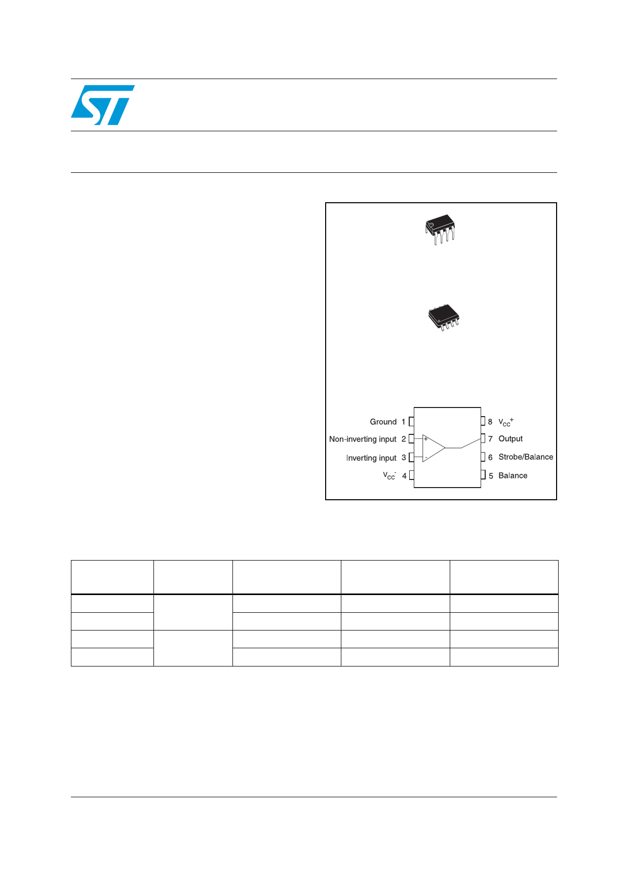
N
DIP8
(Plastic package)
D
SO-8
(Plastic micropackage)
Pin connections (top view)
Order codes
Part number
LM211N
LM211D/DT
LM311N
LM311D/DT
Temperature
range
-40°C, +105°C
0°C, +70°C
Package
DIP8
SO-8
DIP8
SO-8
Packing
Tube
Tube or tape & reel
Tube
Tube or Tape & reel
Marking
LM211N
211
LM311
311
September 2006
Rev 4
1/14
www.st.com
14
1 page 
LM111-LM211-LM311
3 Electrical characteristics
Electrical characteristics
Table 3.
Symbol
VCC+ = ±15V, Tamb = +25°C (unless otherwise specified)
Parameter
Conditions
LM111 - LM211
Min. Typ. Max.
LM311
Min. Typ. Max.
Unit
Vio
Iio
Iib
Avd
ICC+
ICC-
Input offset voltage (1)
Input offset current (1)
Input bias current (1)
Large signal voltage gain
RS ≤ 50kΩ
Tamb = +25°C
Tmin ≤ Tamb ≤ Tmax
Tamb = +25°C
Tmin ≤ Tamb ≤ Tmax
Tamb = +25°C
Tmin ≤ Tamb ≤ Tmax
Supply currents
Positive
Negative
0.7 3
4
4 10
20
60 100
150
2 7.5 mV
10
6
50
70
nA
100 250
300
nA
40 200
40 200
V/mV
5.1 6
4.1 5
5.1
4.1
7.5
5
mA
Vicm
Input common mode
voltage range
VOL Low level output voltage
IOH High level output current
Istrobe
tre
Strobe current
Response time (2)
Tmin ≤ Tamb ≤ Tmax
-14.5 +13.8 +13 -14.5 +13.8 +13
-14.7
-14.7
Tamb = +25°C, IO = 50mA,
Vi ≤-5mV
0.75 1.5
Tamb = +25°C, IO = 50mA,
Vi ≤-10mV
0.75 1.5
Tmin ≤ Tamb ≤ Tmax
VCC+ ≥ +4.5V, VCC- = 0
IO = 8mA, Vi ≤-6m
0.23 0.4
Tmin ≤ Tamb ≤ Tmax
VCC+ ≥ +4.5V, VCC- = 0
IO = 8mA, Vi ≤ -10mV
0.23 0.4
Tamb = +25°C
Vi ≥ +5mV, VO = +35V
0.2 10
Tamb = +25°C
Vi ≥ +10mV, VO = +35V
0.2 50
Tmin ≤ Tamb ≤ Tmax
Vi ≥ +5mV, VO = +35V
0.1 0.5
33
V
V
nA
nA
µA
mA
200 200 ns
1. The offset voltage, offset current and bias current specifications apply for any supply voltage from a single +5V supply up to
±15V supplies. The offset voltages and offset currents given are the maximum values required to drive the output down to
+1V or up to +14V with a 1mA load current. Thus, these parameters define an error band and take into account the worst-
case of voltage gain and input impedance.
2. The response time specified is for a 100mV input step with 5mV overdrive.
5/14
5 Page 
LM111-LM211-LM311
5.1 DIP8 package
Package mechanical data
DIM.
A
a1
B
B1
b
b1
D
E
e
e3
e4
F
I
L
Z
Plastic DIP-8 MECHANICAL DATA
MIN.
0.7
1.39
0.91
0.38
0.44
mm.
TYP
3.3
0.5
8.8
2.54
7.62
7.62
3.3
MAX.
1.65
1.04
0.5
9.8
MIN.
0.028
0.055
0.036
0.015
7.1
4.8
1.6 0.017
inch
TYP.
0.130
0.020
0.346
0.100
0.300
0.300
0.130
MAX.
0.065
0.041
0.020
0.386
0.280
0.189
0.063
P001F
11/14
11 Page | ||
| Páginas | Total 14 Páginas | |
| PDF Descargar | [ Datasheet LM311.PDF ] | |
Hoja de datos destacado
| Número de pieza | Descripción | Fabricantes |
| LM310 | Voltage Follower | National Semiconductor |
| LM3100 | LM3100 SIMPLE SWITCHER Synchronous 1MHz 1.5A Step-Down Voltage Regulator (Rev. G) | Texas Instruments |
| LM3100 | Voltage Regulator | National Semiconductor |
| LM3102 | LM3102/-Q1 SIMPLE SWITCHER Synchronous 1-MHz 2.5-A Step-Down Voltage Regulator (Rev. H) | Texas Instruments |
| Número de pieza | Descripción | Fabricantes |
| SLA6805M | High Voltage 3 phase Motor Driver IC. |
Sanken |
| SDC1742 | 12- and 14-Bit Hybrid Synchro / Resolver-to-Digital Converters. |
Analog Devices |
|
DataSheet.es es una pagina web que funciona como un repositorio de manuales o hoja de datos de muchos de los productos más populares, |
| DataSheet.es | 2020 | Privacy Policy | Contacto | Buscar |