|
|
|
PDF LM2903A Data sheet ( Hoja de datos )
| Número de pieza | LM2903A | |
| Descripción | DUAL AND QUAD DIFFERENTIAL COMPARATORS | |
| Fabricantes | Diodes | |
| Logotipo | ||
Hay una vista previa y un enlace de descarga de LM2903A (archivo pdf) en la parte inferior de esta página. Total 18 Páginas | ||
|
No Preview Available !
LM2901/ LM2901A/ LM2903/ LM2903A
DUAL AND QUAD DIFFERENTIAL COMPARATORS
Description
The LM2901/2903 series comparators consist of four and two
independent precision voltage comparators with very low input offset
voltage specification. They are designed to operate from a single
power supply over a wide range of voltages; however operation from
split power supplies is also possible. They offer low power supply
current independent of the magnitude of the power supply voltage.
The LM2901/2903 series comparators are designed to directly
interface with TTL and CMOS. When operating from both plus and
minus power supplies, the LM2901/2903 series comparators will
directly interface with MOS logic where their low power drain is a
distinct advantage over standard comparators.
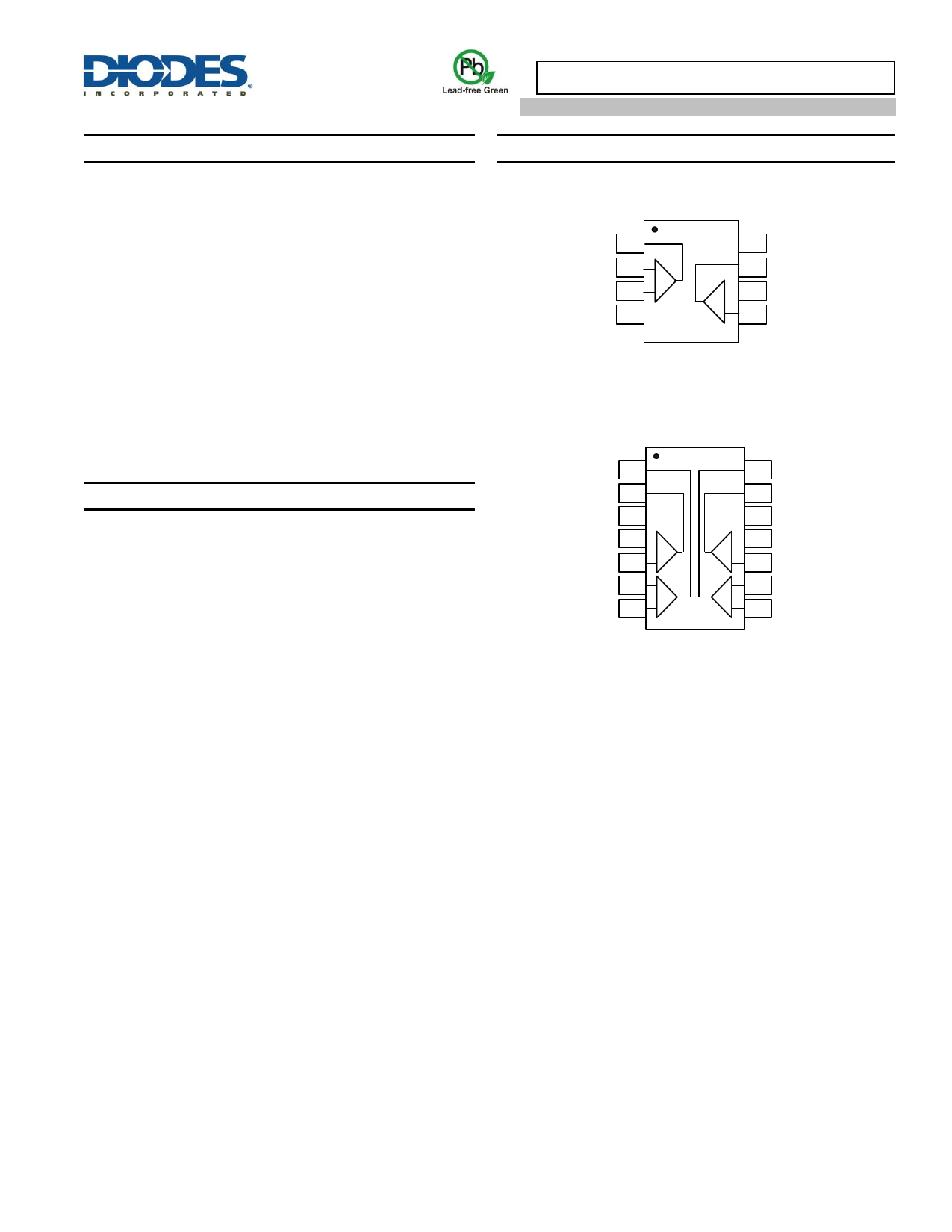
Pin Assignments
(Top View)
1OUT
1IN-
1IN+
GND
1
2
3
4
-
1
8 VCC
7 2OUT
6 2IN-
2
- 5 2IN+
SO-8/TSSOP-8/MSOP-8
LM2903/ LM2903A
The dual devices are available in SO-8, TSSOP-8, MSOP-8 and the
quad devices available in SO-14 and TSSOP-14 with industry
standard pinouts. Both use green mold compound as standard.
(Top View)
1OUT 1
14 3OUT
Features
Wide Power Supply Range:
Single Supply: 2V to 36V
Dual Supplies: ±1.0V to ±18V
Very Low Supply Current Drain – Independent of Supply Voltage
LM2903: 0.6mA
LM2901: 0.9mA
2OUT 2
VCC 3
2IN- 4
2IN+ 5
1IN- 6
1IN+ 7
-
2
-
1
13 4OUT
12 GND
11 4IN+
4
- 10 4IN-
9 3IN+
3
- 8 3IN-
Low Input Bias Current: 25nA
Low Input Offset Current: ±5nA
Typical Offset Voltage:
Non-A Device: 2mV
A Device: 1mV
SO-14/TSSOP-14
LM2901/ LM2901A
Common-Mode Input Voltage Range Includes Ground
Differential Input Voltage Range Equal to the Power Supply
Voltage
Low Output Saturation Voltage:
LM2903: 200mV at 4mA
LM2901: 100mV at 4mA
Output Voltage Compatible with TTL, MOS and CMOS
Totally Lead-Free & Fully RoHS Compliant (Notes 1 & 2)
Halogen and Antimony Free. “Green” Device (Note 3)
Notes:
1. No purposely added lead. Fully EU Directive 2002/95/EC (RoHS) & 2011/65/EU (RoHS 2) compliant.
2. See http://www.diodes.com/quality/lead_free.html for more information about Diodes Incorporated’s definitions of Halogen- and Antimony-free, "Green"
and Lead-free.
3. Halogen- and Antimony-free "Green” products are defined as those which contain <900ppm bromine, <900ppm chlorine (<1500ppm total Br + Cl) and
<1000ppm antimony compounds.
LM2901/ LM2901A/ LM2903/ LM2903A
Document number: DS36779 Rev. 3 - 2
1 of 18
www.diodes.com
May 2016
© Diodes Incorporated
1 page 
LM2901/ LM2901A/ LM2903/ LM2903A
Electrical Characteristics (Notes 8 & 9) (@VCC = 5.0V, GND = 0V, TA = +25°C, unless otherwise specified.)
LM2903, LM2903A
Parameter
VIO Input Offset Voltage
IB Input Bias Current
IIO Input Offset Current
Conditions
VIC = VCMR Min,
VO = 1.4V,
VCC = 5V to =30V
(Note 10)
Non-A Device
A-Suffix Device
IIN+ or IIN− with OUT in Linear Range,
VCM = 0V (Note 11)
IIN+ - IIN−, VCM = 0V
VCMR
Input Common-Mode Voltage
Range
VCC = 30V (Note 12)
ICC Supply Current
RL = ∞ on
Both Channels
VCC = 30V
VCC = 5V
AV
—
—
IO(SINK)
VSAT
Voltage Gain
Large Signal Response Time
Response Time
Output Sink Current
Saturation Voltage
VCC = 15V, VOUT = 1V to 11V,
RL ≥ 15kΩ,
VIN = TTL Logic Swing, VREF = 1.4V,
VRL = 5V, RL = 5.1kΩ
VRL = 5V, RL = 5.1kΩ (Note 13)
VIN− = 1V, VIN+ = 0, VO ≤ 1.5V
VIN− = 1V, VIN+ = 0, ISINK ≤ 4mA
IO(LEAK) Output Leakage Current
VID Differential Input Voltage
VIN− = 0V, VIN+ = 1, VO = 5V
VIN− = 0V, VIN+ = 1, VO = 30V
All VIN ≥0V (or V- if used) (Note 14)
TA
TA = +25°C
Full Range
TA = +25°C
Full Range
TA = +25°C
Full Range
TA = +25°C
Full Range
TA = +25°C
Full Range
TA = +25°C
Full Range
TA = +25°C
Full Range
Min
—
—
—
—
—
—
—
—
0 to
VCC -1.5
0 to
VCC-2
—
—
—
—
TA = +25°C
50
TA = +25°C
TA = +25°C
TA = +25°C
TA = +25°C
Full Range
TA = +25°C
Full Range
Full Range
—
—
6
—
—
—
—
—
Typ
2
—
1
—
25
—
5
—
—
—
0.7
—
0.6
—
200
300
1.3
16
200
—
0.1
—
—
Max
7
15
2
4
250
500
50
200
—
—
Unit
mV
nA
nA
V
1.7
3.0
mA
1
2.0
— V/mV
— ns
— µs
— mA
400
mV
700
— nA
1 µA
36 V
Notes:
8. Typical values represent the most likely parametric norm as determined at the time of characterization. Actual typical values may vary over time and
will also depend on the application and configuration. The typical values are not tested and are not guaranteed
on shipped production material.
9. All limits are guaranteed by testing or statistical analysis. Limits over the full temperature are guaranteed by design, but not tested in production.
10. VO 1.4V, RS = 0Ω with VCC from 5V to 30V;
11. The direction of the input current is out of the IC due to the PNP input stage. This current is essentially constant, independent of the state of the
output so no loading change exists on the input lines.
12. The input common-mode voltage of either input signal voltage should not be allowed to go negative by more than 0.3V (@ +25°C). The upper end of
the common-mode voltage range is VCC -1.5V (@ +25°C), but either or both inputs can go to +36V without damage, independent of the magnitude of VCC.
13. The response time specified is for a 100mV step input with 5mV overdrive. For larger overdrive signals 300ns can be obtained, see typical
performance characteristics.
14. Positive excursions of input voltage may exceed the power supply level. As long as other voltages remain within the common mode range, the
comparator will provide a proper output stage. The low voltage state must not be less than -0.3V (or 0.3V below the magnitude of the negative power
supply, if used).
LM2901/ LM2901A/ LM2903/ LM2903A
Document number: DS36779 Rev. 3 - 2
5 of 18
www.diodes.com
May 2016
© Diodes Incorporated
5 Page 
LM2901/ LM2901A/ LM2903/ LM2903A
Typical Application Circuit (VCC = 5.0VDC) (Cont.)
V+(12VDC)
+VREF HIGH
2RS
+
10KΩ
+
VIN
RS
-
+
+VREF LOW
2RS
-
Limit Comparator
V+
LAMP
12 ESB
2N2222
+ 3.0KΩ
VO
-
+
-
ORing the Outputs
V+
100pF
+
0
t0
1N914
1MΩ
-
1MΩ
+
0.001uF
1MΩ
1N914
10KΩ
Vo
1ms
PW
t0 t1
V+
0
One-Shot Multivibrator
+VIN1
-VIN2
2N2222
100KΩ
100KΩ
5.1KΩ
Comparing Input Voltage of
Opposite Polarity
V+
V+
0
“0”"1”
5.1KΩ
100KΩ
VIN
1N914
5.1KΩ
100KΩ
-
+
20MΩ
10KΩ
5.1KΩ
Vo
Zero Crossing Detector
(Single Power Supply)
75pF
100KΩ
V+
100KΩ
100KΩ
-
+
100KΩ
V+
4.3KΩ
V+
0
1:100KHz
Vo
Squarewave Oscillator
LM2901/ LM2901A/ LM2903/ LM2903A
Document number: DS36779 Rev. 3 - 2
11 of 18
www.diodes.com
May 2016
© Diodes Incorporated
11 Page | ||
| Páginas | Total 18 Páginas | |
| PDF Descargar | [ Datasheet LM2903A.PDF ] | |
Hoja de datos destacado
| Número de pieza | Descripción | Fabricantes |
| LM2903 | LOW POWER DUAL VOLTAGE COMPARATORS | STMicroelectronics |
| LM2903 | Dual Differential Comparator | Fairchild Semiconductor |
| LM2903 | Low power dual voltage comparator | NXP Semiconductors |
| LM2903 | Low Offset Voltage Dual Comparators | ON Semiconductor |
| Número de pieza | Descripción | Fabricantes |
| SLA6805M | High Voltage 3 phase Motor Driver IC. |
Sanken |
| SDC1742 | 12- and 14-Bit Hybrid Synchro / Resolver-to-Digital Converters. |
Analog Devices |
|
DataSheet.es es una pagina web que funciona como un repositorio de manuales o hoja de datos de muchos de los productos más populares, |
| DataSheet.es | 2020 | Privacy Policy | Contacto | Buscar |