|
|
|
PDF KB3511 Data sheet ( Hoja de datos )
| Número de pieza | KB3511 | |
| Descripción | Step-Down DC/DC Converter | |
| Fabricantes | Kingbor Technology | |
| Logotipo | ||
Hay una vista previa y un enlace de descarga de KB3511 (archivo pdf) en la parte inferior de esta página. Total 14 Páginas | ||
|
No Preview Available !
Kingbor Technology Co.,Ltd
TEL:(86)0755-26508846 FAX:(86)0755-26509052
KB3511
System-Power
High Efficiency, Low Noise, Fast Transient
Dual 800mA, 2.2MHz Step-Down DC/DC Converter
FEATURES
■ Up to 97% Efficiency
■ 25uA No Load Current Per Channel
www.Data■She8e0t40Um.cAomOutput Current
■ 2.5V to 6.5V Input Voltage Range
■ 2.2MHz Constant Frequency Operation
■ No Schottky Diode Required
■ Low Dropout Operation: 100% Duty Cycle
■ 0.6V Reference Allows Low Output Voltages
■ Shutdown Mode Draws ) 1µA Supply Current
■ Current Mode Operation for Excellent Line and
Load Transient Response
■ Overtemperature Protected
■ DFN33-10 Package
APPLICATIONS
■ Cellular Telephones
■ Personal Information Appliances
■ Wireless and DSL Modems
■ Digital Still Cameras
■ MP3 Players
■ Portable Instruments
DESCRIPTION
The KB3511 is a high efficiency monolithic synchro-
nous buck regulator using a constant frequency, current
mode architecture. The device is available in an adjustable
version and fixed output voltages of 1.8V and 3.3V. Supply
current during operation is only 25µA and drops to )1µA
in shutdown. The 2.5V to 6.5V input voltage range makes
the KB3511 ideally suited for single Li-Ion battery-pow-
ered applications. 100% duty cycle provides low dropout
operation, extending battery life in portable systems.
Automatic Trickle Mode operation increases efficiency at
light loads, further extending battery life.
Switching frequency is internally set at 2.2MHz, allowing
the use of small surface mount inductors and capacitors.
The internal synchronous switch increases efficiency and
eliminates the need for an external Schottky diode. Low
output voltages are easily supported with the 0.6V feed-
back reference voltage. The KB3511 is available in a low
profile (0.8mm) DFN33-10 package.
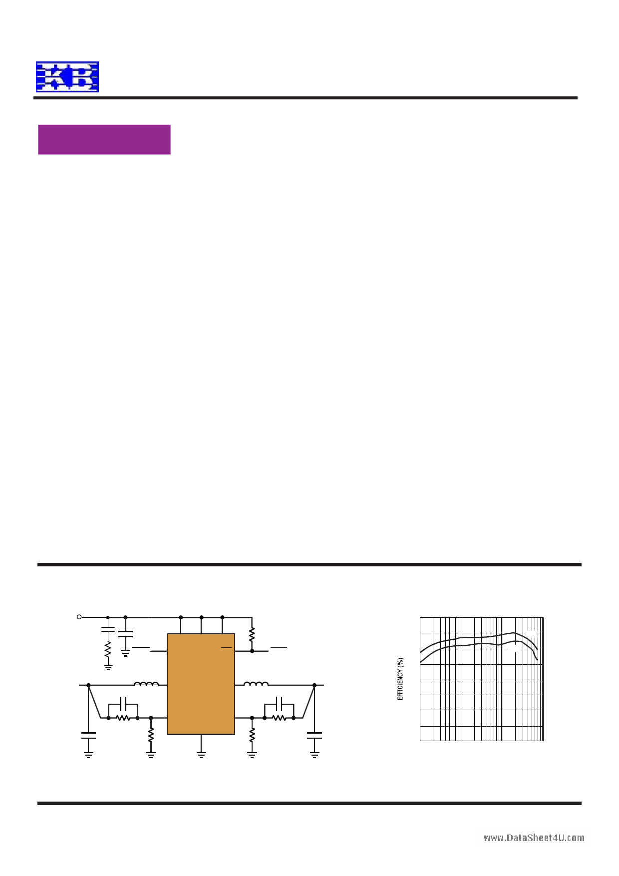
TYPICAL APPLICATION
VIN = 3.6V
TO 6.0V
C6
*10µ F
* Vin>4.5V Used R1
*1
VOUT2 = 3.3V
AT 800mA
C1
4.7µF
RESET
L2
2.2µH
C5, 22pF
23
RUN1 VIN
6 MODE/SYNC
9
RUN2
POR 8
KB3511A
4 SW1
SW2 7
DFN3x3mm
R5
100k
RESET
L1
2.2µH
C4, 22pF
C3
4.7µF
R4
680k R3
150k
1
VFB1
GND
11 5
VFB2 10
R2
R1 300k
150k
VOUT1 = 1.8V
AT 800mA
C2
4.7µF
C1, C2, C3: 4.7uF 6.3V 0603
L1, L2: EVERCOM SD11-2R2 (3x3x1.2mm)
Figure 1. 3.3V/1.8V at 800mA Step-Down Regulators
1.3mm Height Core Supply
KB3511 Efficiency Curve
VIN=3.6V
100
95 3.3V
90 1.8V
85
80
75
70
65
60
1
10 100 1000
LOAD CURRENT (mA)
1
1 page 
Kingbor Technology Co.,Ltd
TEL:(86)0755-26508846 FAX:(86)0755-26509052
PIN FUNCTIONS
KB3511
VFB1 (Pin 1): Output Feedback. Receives the feedback
voltage from the external resistive divider across the
output. Nominal voltage for this pin is 0.6V.
RUN1 (Pin 2): Regulator 1 Enable. Forcing this pin to VIN
enables regulator 1, while forcing it to GND causes regu-
www.DatalSahtoeert41Ut.ocosmhut down.
VIN (Pin 3): Main Power Supply. Must be closely decoupled
to GND.
be syncronized to an external oscillator applied to this pin
and pulse skipping mode is automatically selected.
SW2 (Pin 7): Regulator 2 Switch Node Connection to the
Inductor. This pin swings from VIN to GND.
POR (Pin 8): Power-On Reset . This common-drain logic
output is pulled to GND when the output voltage is not
within ±8.5% of regulation and goes high after 175ms
when both channels are within regulation.
SW1 (Pin 4): Regulator 1 Switch Node Connection to the
Inductor. This pin swings from VIN to GND.
GND (Pin 5): Main Ground. Connect to the (–) terminal of
COUT, and (–) terminal of CIN.
MODE/SYNC (Pin 6): Combination Mode Selection and
Oscillator Synchronization. This pin controls the operation
of the device. When tied to VIN or GND, Trickle Mode
operation or PWM mode is selected, respectively.
Do not float this pin. The oscillation frequency can
RUN2 (Pin 9): Output Feedback. Forcing this pin to VIN
enables regulator 2, while forcing it to GND causes regu-
lator 2 to shut down.
VFB2 (Pin 10): Output Feedback. Receives the feedback
voltage from the external resistive divider across the
output. Nominal voltage for this pin is 0.6V.
Exposed Pad (GND) (Pin 11): Power Ground. Connect to
the (–) terminal of COUT, and (–) terminal of CIN. Must be
soldered to electrical ground on PCB.
5
5 Page 
Kingbor Technology Co.,Ltd
TEL:(86)0755-26508846 FAX:(86)0755-26509052
KB3511
APPLICATIONS INFORMATION
produce the most improvement. Percent efficiency can be
expressed as:
%Efficiency = 100% - (L1 + L2 + L3 + ...)
where L1, L2, etc. are the individual losses as a percentage
of input power.
www.DataSAhlteheot4uUg.chomall dissipative elements in the circuit produce
losses, 4 main sources usually account for most of the
losses in KB3511 circuits: 1)VIN quiescent current, 2)
switching losses, 3) I2R losses, 4) other losses.
1) The VIN current is the DC supply current given in the
Electrical Characteristics which excludes MOSFET driver
and control currents. VIN current results in a small (<0.1%)
loss that increases with VIN, even at no load.
2) The switching current is the sum of the MOSFET driver
and control currents. The MOSFET driver current results
from switching the gate capacitance of the power MOSFETs.
Each time a MOSFET gate is switched from low to high to
low again, a packet of charge dQ moves from VIN to
ground. The resulting dQ/dt is a current out of VIN that is
typically much larger than the DC bias current. In continu-
ous mode, IGATECHG = fO(QT + QB), where QT and QB are the
gate charges of the internal top and bottom MOSFET
switches. The gate charge losses are proportional to VIN
and thus their effects will be more pronounced at higher
supply voltages.
3) I2R losses are calculated from the DC resistances of the
internal switches, RSW, and external inductor, RL. In
continuous mode, the average output current flowing
through inductor L, but is “chopped” between the internal
top and bottom switches. Thus, the series resistance
looking into the SW pin is a function of both top and
bottom MOSFET RDS(ON) and the duty cycle (DC) as
follows:
RSW = (RDS(ON)TOP)(DC) + (RDS(ON)BOT)(1 – DC)
The RDS(ON) for both the top and bottom MOSFETs can be
obtained from the Typical Performance Characteristics
curves. Thus, to obtain I2R losses:
I2R losses = IOUT2(RSW + RL)
4) Other ‘hidden’ losses such as copper trace and internal
battery resistances can account for additional efficiency
degradations in portable systems. It is very important to
include these “system” level losses in the design of a
system. The internal battery and fuse resistance losses
can be minimized by making sure that CIN has adequate
charge storage and very low ESR at the switching fre-
quency. Other losses including diode conduction losses
during dead-time and inductor core losses generally ac-
count for less than 2% total additional loss.
Thermal Considerations
In a majority of applications, the KB3511 does not
dissipate much heat due to its high efficiency. However, in
applications where the KB3511 is running at high ambi-
ent temperature with low supply voltage and high duty
cycles, such as in dropout, the heat dissipated may exceed
the maximum junction temperature of the part. If the
junction temperature reaches approximately 150°C, both
power switches will be turned off and the SW node will
become high impedance.
To prevent the KB3511 from exceeding the maximum
junction temperature, the user will need to do some
thermal analysis. The goal of the thermal analysis is to
determine whether the power dissipated exceeds the
maximum junction temperature of the part. The tempera-
ture rise is given by:
TRISE = PD • θJA
where PD is the power dissipated by the regulator and θJA
is the thermal resistance from the junction of the die to the
ambient temperature.
The junction temperature, TJ, is given by:
TJ = TRISE + TAMBIENT
As an example, consider the case when the KB3511 is in
dropout on both channels at an input voltage of 2.7V with
a load current of 800mA and an ambient temperature of
70°C. From the Typical Performance Characteristics graph
of Switch Resistance, the RDS(ON) resistance of the main
switch is 0.425Ω. Therefore, power dissipated by each
channel is:
PD = I2 • RDS(ON) = 272mW
The MS package junction-to-ambient thermal resistance,
θJA, is 45°C/W. Therefore, the junction temperature of the
11
11 Page | ||
| Páginas | Total 14 Páginas | |
| PDF Descargar | [ Datasheet KB3511.PDF ] | |
Hoja de datos destacado
| Número de pieza | Descripción | Fabricantes |
| KB3511 | Step-Down DC/DC Converter | Kingbor Technology |
| Número de pieza | Descripción | Fabricantes |
| SLA6805M | High Voltage 3 phase Motor Driver IC. |
Sanken |
| SDC1742 | 12- and 14-Bit Hybrid Synchro / Resolver-to-Digital Converters. |
Analog Devices |
|
DataSheet.es es una pagina web que funciona como un repositorio de manuales o hoja de datos de muchos de los productos más populares, |
| DataSheet.es | 2020 | Privacy Policy | Contacto | Buscar |