|
|
|
PDF ZL10100 Data sheet ( Hoja de datos )
| Número de pieza | ZL10100 | |
| Descripción | Single Chip Synthesized Downconverter | |
| Fabricantes | Zarlink Semiconductor | |
| Logotipo | ||
Hay una vista previa y un enlace de descarga de ZL10100 (archivo pdf) en la parte inferior de esta página. Total 19 Páginas | ||
|
No Preview Available !
ZL10100
Single Chip Synthesized
Downconverter with IF Amplifier
Data Sheet
Features
• Single chip synthesised downconverter forming a
complete double conversion tuner when
combined with the SL2100 or SL2101
• Compatible with digital and analogue system
requirements
• CTB contribution < -64 dBc, CXM contribution
< -62 dBc and spectral spread < -64 dBc
www.DataShee•t4UIS.FcAomaWmfpilltiefiresr optimized to interface with standard
• Extremely low phase noise balanced local
oscillator, with very low fundamental and
harmonic radiation
• PLL frequency synthesizer designed for high
comparison frequencies and low phase noise
• Available in 28 pin SSOP and MLP packages
Applications
• Double conversion tuners
• Digital Terrestrial tuners
• Cable Modems
• Cable telephony
• MATV
April 2005
Ordering Information
ZL10100/DDE
ZL10100/DDF
ZL10100/DDE1
ZL10100/DDF1
ZL10100/LDG1
ZL10100/LDF1
SSOP
SSOP
SSOP*
SSOP*
MLP*
MLP*
Tubes
Tape & Reel,
Tubes
Tape & Reel
Trays
Tape & Reel
* Pb free
All codes Baked an Drypacked
-40°C to +85°C
Description
The ZL10100 is a fully integrated single chip mixer
oscillator with on-board low phase noise I2C bus
controlled PLL frequency synthesizer. It is intended
primarily as the down converter for application in
double conversion tuners and is compatible with HIIF
frequencies between 1 and 1.3 GHz and all standard
tuner IF output frequencies.
The device contains all elements necessary, with the
exception of local oscillator tuning network, loop filter
and crystal reference to fabricate a complete
synthesized block converter with IF amplifier,
compatible with digital and analogue requirements.
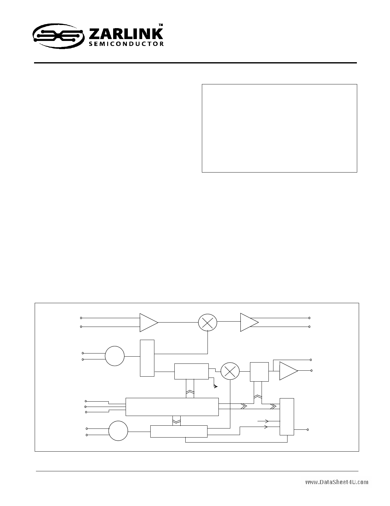
RF Input
RF InputB
IF Output
IF OutputB
LO
LOB
VCO
SDA
SCL
ADD
XTAL
XTALCAP
REF
OSC
15 Bit
Programmable
Divider
fp2d/
I2C Bus
Interface
Reference Divider
CPhuamrgpe
Fpd/2
Fcomp
Pump
Drive
Port P0
Figure 1 - ZL10100 Functional Block Diagram
1
Zarlink Semiconductor Inc.
Zarlink, ZL and the Zarlink Semiconductor logo are trademarks of Zarlink Semiconductor Inc.
Copyright 2002-2005, Zarlink Semiconductor Inc. All Rights Reserved.
1 page 
ZL10100
Data Sheet
The typical application for the crystal oscillator is contained in Figure 9 which also demonstrates how a 4 MHz
reference signal can be coupled out to a further PLL frequency synthesizer, such as the upconverter section in a
double conversion tuner.
The output of the phase detector feeds a charge pump and loop amplifier, which when used with an external loop
filter and high voltage transistor, integrates the current pulses into the varactor line voltage, used for controlling the
oscillator.
The programmable divider output Fpd divided by two and the reference divider output Fcomp can be switched to
port P0 by programming the device into test mode. The test modes are described in Table 2.
2.0 Programming
The ZL10100 is controlled by an I2C data bus and is compatible with both standard and fast mode formats.
www.DataSheet4U.com
Data and Clock are fed in on the SDA and SCL lines respectively as defined by I2C bus format. The device can
either accept data (write mode), or send data (read mode). The LSB of the address byte (R/W) sets the device into
write mode if it is low, and read mode if it is high. Tables 3, 4 and 5 illustrate the format of the data. The device can
be programmed to respond to several addresses, which enables the use of more than one device in an I2C bus
system. Table 5 shows how the address is selected by applying a voltage to the 'ADD' input. When the device
receives a valid address byte, it pulls the SDA line low during the acknowledge period, and during following
acknowledge periods after further data bytes are received. When the device is programmed into read mode, the
controller accepting the data must pull the SDA line low during all status byte acknowledge periods to read another
status byte. If the controller fails to pull the SDA line low during this period, the device generates an internal STOP
condition, which inhibits further reading.
2.1 Write Mode
With reference to Table 5, bytes 2 and 3 contain frequency information bits 214-20 inclusive. Byte 4 controls the
synthesizer reference divider ratio, see Table 1 and the charge pump setting, see Table 6. Byte 5 controls the test
modes, see Table 2 and the output port P0.
After reception and acknowledgement of a correct address (byte 1), the first bit of the following byte determines
whether the byte is interpreted as a byte 2 or 4, a logic '0' indicating byte 2, and a logic '1' indicating byte 4. Having
interpreted this byte as either byte 2 or 4 the following data byte will be interpreted as byte 3 or 5 respectively.
Having received two complete data bytes, additional data bytes can be entered, where byte interpretation follows
the same procedure, without re-addressing the device. This procedure continues until a STOP condition is
received. The STOP condition can be generated after any data byte, if however it occurs during a byte
transmission, the previous byte data is retained. To facilitate smooth fine tuning, the frequency data bytes are only
accepted by the device after all 15 bits of frequency data have been received, or after the generation of a STOP
condition.
2.2 Read Mode
When the device is in read mode, the status byte read from the device takes the form shown in Table 4.
Bit 1 (POR) is the power-on reset indicator, and this is set to a logic '1' if the Vcc supply to the device has dropped
below 3 V (at 25°C), e.g., when the device is initially turned ON. The POR is reset to '0' when the read sequence is
terminated by a STOP command. When POR is set high this indicates that the programmed information may have
been corrupted and the device reset to the power up condition.
Bit 2 (FL) indicates whether the synthesizer is phase locked, a logic '1' is present if the device is locked, and a logic
'0' if the device is unlocked.
5
Zarlink Semiconductor Inc.
5 Page 
ZL10100
Data Sheet
C1 C0
Current in µA
Min.
Typ.
Max.
0
0 ± 98
± 130 ± 162
0 1 ± 210 ± 280 ± 350
1 0 ± 450 ± 600 ± 750
1 1 ± 975 ± 1300 ± 1625
Table 6 - Charge Pump Current
Electrical Characteristics - Test conditions (unless otherwise stated)
Tamb = -40°C to 85°C, Vee = 0 V, Vcc = 5 V±5%. Input frequency 1220 MHz. IF output frequency 44 MHz.
These characteristics are guaranteed by either production test or design. They apply within the specified ambient temperature and supply
voltage unless otherwise stated.
Characteristic
www.DataSheet4U.com
Supply current
Pin Min. Typ. Max. Units
120 160
mA
Conditions
Input frequency range
1 1.3 GHz
Composite peak input signal
86 dBµV Operating condition only.
Input impedance
See Figure 4.
Input Noise Figure
9 11 dB Tamb = 27°C
Conversion gain
20 23 26
dB Differential to differential
voltage gain to differential
150 Ω load.
Gain variation within channel
0.5 dB Channel bandwidth 8 MHz
within operating frequency
range.
Through gain
-30 dB
CTB
-64 dBc See note 4.
CXM
-62 dBc See note 4.
LO operating range
0.9 1.6 GHz Maximum tuning range
determined by application,
see note (3), guaranteed by
design.
LO phase noise, SSB
@ 10 kHz offset
@ 100 kHz offset
-94
-116
-90
-110
See Figure 7.
dBc/Hz Application as in Figure 6.
dBc/Hz
LO phase noise floor
-136 dBc/Hz Application as in Figure 6.
IF output frequency range
30 60 MHz
IF output impedance
75 Ω Single-ended. See Figure 8.
IF output return loss
-20 dB See Figure 8, over operating
range.
All other spurs on IF Output
20 dBµV Within channel bandwidth of
8 MHz.
11
Zarlink Semiconductor Inc.
11 Page | ||
| Páginas | Total 19 Páginas | |
| PDF Descargar | [ Datasheet ZL10100.PDF ] | |
Hoja de datos destacado
| Número de pieza | Descripción | Fabricantes |
| ZL10100 | Single Chip Synthesized Downconverter | Zarlink Semiconductor |
| Número de pieza | Descripción | Fabricantes |
| SLA6805M | High Voltage 3 phase Motor Driver IC. |
Sanken |
| SDC1742 | 12- and 14-Bit Hybrid Synchro / Resolver-to-Digital Converters. |
Analog Devices |
|
DataSheet.es es una pagina web que funciona como un repositorio de manuales o hoja de datos de muchos de los productos más populares, |
| DataSheet.es | 2020 | Privacy Policy | Contacto | Buscar |