|
|
|
PDF AD9020 Data sheet ( Hoja de datos )
| Número de pieza | AD9020 | |
| Descripción | 10-Bit 60 MSPS A/D Converter | |
| Fabricantes | Analog Devices | |
| Logotipo | ||
Hay una vista previa y un enlace de descarga de AD9020 (archivo pdf) en la parte inferior de esta página. Total 12 Páginas | ||
|
No Preview Available !
a
10-Bit 60 MSPS
A/D Converter
AD9020
FEATURES
Monolithic 10-Bit/60 MSPS Converter
TTL Outputs
Bipolar (؎1.75 V) Analog Input
56 dB SNR @ 2.3 MHz Input
Low (45 pF) Input Capacitance
MIL-STD-883-Compliant Versions Available
APPLICATIONS
Digital Oscilloscopes
Medical Imaging
Professional Video
Radar Warning/Guidance Systems
Infrared Systems
GENERAL DESCRIPTION
The AD9020 A/D converter is a 10-bit monolithic converter
capable of word rates of 60 MSPS and above. Innovative archi-
tecture using 512 input comparators instead of the traditional
1024 required by other flash converters reduces input capaci-
tance and improves linearity.
Encode and outputs are TTL-compatible, making the AD9020
an ideal candidate for use in low power systems. An over-
flow bit is provided to indicate analog input signals greater
than +VSENSE.
Voltage sense lines are provided to insure accurate driving of the
± VREF voltages applied to the units. Quarter-point taps on the
resistor ladder help optimize the integral linearity of the unit.
Either 68-pin ceramic leaded (gull wing) packages or ceramic
LCCs are available and are specifically designed for low thermal
impedances. Two performance grades for temperatures of both
0°C to 70°C and –55°C to +125°C ranges are offered to allow
the user to select the linearity best suited for each application.
Dynamic performance is fully characterized and production
tested at 25°C. MIL-STD-883 units are available.
The AD9020 A/D Converter is available in versions compliant
with MIL-STD-883. Refer to the Analog Devices Military Prod-
ucts Databook or current AD9020/883B data sheet for detailed
specifications.
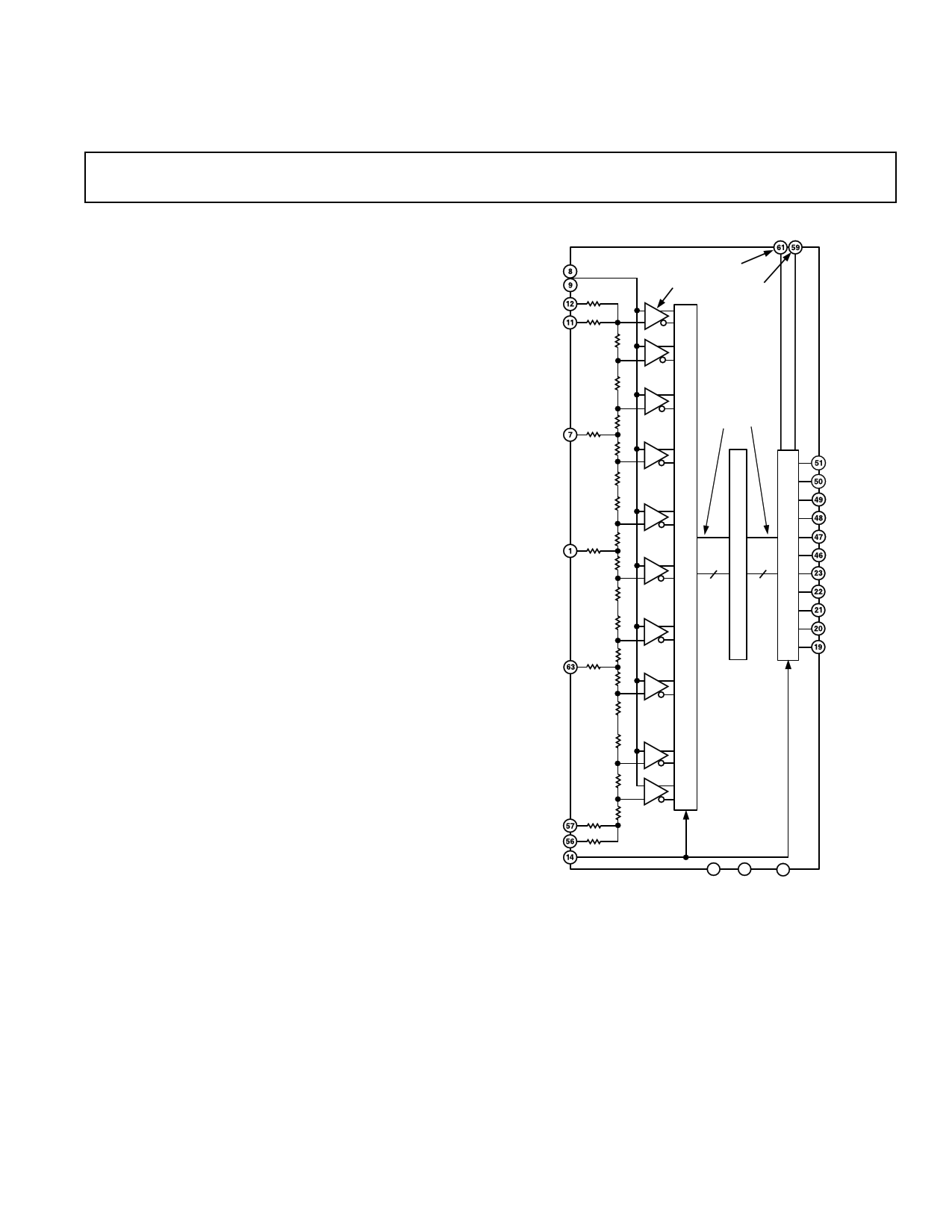
FUNCTIONAL BLOCK DIAGRAM
ANALOG IN
+VREF
+VSENSE
3/4REF
1/2REF
1/4REF
–VSENSE
–VREF
ENCODE
MSB
INVERT
OVERFLOW
LSBS
INVERT
R/2
512
AD9020
R
385
R/2
OVERFLOW
R/2 384 C
O
RM
PD
R AE
257 R
C
A OL
R/2 T D A
O ET
R/2
256
R 1024
10 C
LH
R LO
AG
T
R 129 C
H
I
C
R/2 E
S
R/2
128
R
R
2
R
1
R/2
OVERFLOW
D9 (MSB)
D8
D7
D6
D5
D4
D3
D2
D1
D0 (LSB)
–VS +VS GROUND
REV. C
Information furnished by Analog Devices is believed to be accurate and
reliable. However, no responsibility is assumed by Analog Devices for its
use, nor for any infringements of patents or other rights of third parties that
may result from its use. No license is granted by implication or otherwise
under any patent or patent rights of Analog Devices.
One Technology Way, P.O. Box 9106, Norwood, MA 02062-9106, U.S.A.
Tel: 781/329-4700
www.analog.com
Fax: 781/326-8703
© Analog Devices, Inc., 2001
1 page 
PIN CONFIGURATION
AD9020
NC
+VSENSE
+VREF
GND
ENCODE
+VS
–VS
GND
+VS
(LSB) D0
D1
D2
D3
D4
NC
+VS
NC
9
10
26
27
AD9020
TOP VIEW
(NOT TO SCALE)
61
60
44
43
NC
LSBs INVERT
NC
–VSENSE
–VREF
+VS
–VS
GND
+VS
OVERFLOW
D9 (MSB)
D8
D7
D6
D5
+VS
NC
NC = NO CONNECT
Pin No.
1
2, 16, 28, 29, 35, 41, 42,
54, 64
3, 6, 15, 18, 25, 30, 33, 34,
37, 40, 45, 52, 55, 65, 68
4, 5, 13, 17, 27, 31, 32,
36, 38, 39, 43, 53, 66, 67
7
8, 9
11
12
14
19–23, 46–50
51
56
57
59
61
63
Name
1/2REF
–VS
PIN FUNCTION DESCRIPTIONS
Function
Midpoint of internal reference ladder.
Negative supply voltage; nominally –5.0 V ± 5%.
+VS Positive supply voltage; nominally 5 V ± 5%.
GROUND
3/4REF
ANALOG IN
+VSENSE
+VREF
ENCODE
D0–D4, D5–D9
OVERFLOW
–VREF
–VSENSE
LSBs INVERT
MSB INVERT
1/4REF
All ground pins should be connected together and to low impedance ground
plane.
Three-quarter point of internal reference ladder.
Analog input; nominally between ± 1.75 V.
Voltage sense line to most positive point on internal resistor ladder.
Normally 1.75 V.
Voltage force connection for top of internal reference ladder. Normally driven
to provide 1.75 V at +VSENSE.
TTL-compatible convert command used to begin digitizing process.
TTL-compatible digital output data.
TTL-compatible output indicating ANALOG IN > +VSENSE.
Voltage force connection for bottom of internal reference ladder. Normally
driven to provide –1.75 V at –VSENSE.
Voltage sense line to most negative point on internal resistor ladder.
Normally –1.75 V.
Normally grounded. When connected to +VS, lower order bits (D0–D8) are
inverted.
Normally grounded. When connected to +VS, most significant bit (MSB; D9)
is inverted.
One-quarter point of internal reference ladder.
REV. C
–5–
5 Page 
62 10.0
ENCODE RATE = 40MSPS
56 9.0
50
25؇C
8.0
44
55؇C & 125؇C
38
7.0
6.0
32 5.0
26 4.0
20
1 10 100 200
INPUT FREQUENCY – MHz
Figure 10. SNR and ENOB vs. Input Frequency
AD9020
62 10.0
56 9.0
ANALOG INPUT = 2.3MHz
50 8.0
44 7.0
38 6.0
32 5.0
26 4.0
20
1 10 100
CONVERSION RATE – MSPS
Figure 12. SNR and ENOB vs. Conversion Rate
30
35
40 125؇C
45
50 –55؇C
25؇C
55
60
65
70
1 10 100
INPUT FREQUENCY – MHz
Figure 11. Harmonics vs. Input Frequency
50
49
RESISTANCE
48
70
60
50
47 40
46
CAPACITANCE
30
45 20
44 10
43
–1.8
–1.2
–0.6
0
0.6
ANALOG INPUT (AIN) – Volts
1.2
0
1.8
Figure 13. Input Capacitance/Resistance vs. Input Voltage
Table I. Truth Table
Step
Range
0 = –1.75 V
FS = +1.75 V
Offset Binary
True
Inverted
MSB INV = “0”
MSB INV = “1”
LSBs INV = “0”
LSBs INV = “1”
Two’s Complement
True
Inverted
MSB INV = “1”
MSB INV = “0”
LSBs INV = “0” LSBs INV = “1”
1024
1023
1022
•
•
•
512
511
510
•
•
•
02
01
00
> +1.7500
+1.7466
+1.7432
•
•
•
+0.0034
0.000
–0.0034
•
•
•
–1.7432
–1.7466
<–1.7466
(1)1111111111
1111111111
1111111110
•
•
•
1000000000
0111111111
0111111110
•
•
•
0000000010
0000000001
0000000000
(1)0000000000
0000000000
0000000001
•
•
•
0111111111
1000000000
1000000001
•
•
•
1111111101
1111111110
1111111111
(1)0111111111
0111111111
0111111110
•
•
•
0000000000
1111111111
1111111110
•
•
•
1000000010
1000000001
1000000000
(1)1000000000
1000000000
1000000001
•
•
•
1111111111
0000000000
0000000001
•
•
•
0111111101
0111111110
0111111111
The overflow bit is always 0 except where noted in parentheses ( ). MSB INVERT and LSBs INVERT are considered dc controls.
REV. C
–11–
11 Page | ||
| Páginas | Total 12 Páginas | |
| PDF Descargar | [ Datasheet AD9020.PDF ] | |
Hoja de datos destacado
| Número de pieza | Descripción | Fabricantes |
| AD9020 | 10-Bit 60 MSPS A/D Converter | Analog Devices |
| AD9022 | 12-Bit 20 MSPS Monolithic A/D Converter | Analog Devices |
| Número de pieza | Descripción | Fabricantes |
| SLA6805M | High Voltage 3 phase Motor Driver IC. |
Sanken |
| SDC1742 | 12- and 14-Bit Hybrid Synchro / Resolver-to-Digital Converters. |
Analog Devices |
|
DataSheet.es es una pagina web que funciona como un repositorio de manuales o hoja de datos de muchos de los productos más populares, |
| DataSheet.es | 2020 | Privacy Policy | Contacto | Buscar |