|
|
|
PDF AD9216 Data sheet ( Hoja de datos )
| Número de pieza | AD9216 | |
| Descripción | Dual A/D Converter | |
| Fabricantes | Analog Devices | |
| Logotipo | ||
Hay una vista previa y un enlace de descarga de AD9216 (archivo pdf) en la parte inferior de esta página. Total 30 Páginas | ||
|
No Preview Available !
FEATURES
Integrated dual 10-bit ADC
Single 3 V supply operation
SNR = 57.6 dBc (to Nyquist, AD9216-105)
SFDR = 74 dBc (to Nyquist, AD9216-105)
Low power: 150 mW/ch at 105 MSPS
Differential input with 300 MHz 3 dB bandwidth
Exceptional crosstalk immunity < -80 dB
Offset binary or twos complement data format
Clock duty cycle stabilizer
APPLICATIONS
Ultrasound equipment
IF sampling in communications receivers
3G, radio point-to-point, LMDS, MMDS
Battery-powered instruments
Hand-held scopemeters
Low cost digital oscilloscopes
GENERAL DESCRIPTION
The AD9216 is a dual, 3 V, 10-bit, 105 MSPS analog-to-digital
converter (ADC). It features dual high performance sample-
and-hold amplifiers (SHAs) and an integrated voltage reference.
The AD9216 uses a multistage differential pipelined archi-
tecture with output error correction logic to provide 10-bit
accuracy and guarantee no missing codes over the full
operating temperature range at up to 105 MSPS data rates.
The wide bandwidth, differential SHA allows for a variety of
user selectable input ranges and offsets, including single-ended
applications. The AD9216 is suitable for various applications,
including multiplexed systems that switch full-scale voltage
levels in successive channels and for sampling inputs at
frequencies well beyond the Nyquist rate.
Dual single-ended clock inputs are used to control all internal
conversion cycles. A duty cycle stabilizer is available on the
AD9216 and can compensate for wide variations in the clock
duty cycle, allowing the converters to maintain excellent
performance. The digital output data is presented in either
straight binary or twos complement format.
Rev. A
Information furnished by Analog Devices is believed to be accurate and reliable.
However, no responsibility is assumed by Analog Devices for its use, nor for any
infringements of patents or other rights of third parties that may result from its use.
Specifications subject to change without notice. No license is granted by implication
or otherwise under any patent or patent rights of Analog Devices. Trademarks and
registered trademarks are the property of their respective owners.
10-Bit, 65/80/105 MSPS
Dual A/D Converter
AD9216
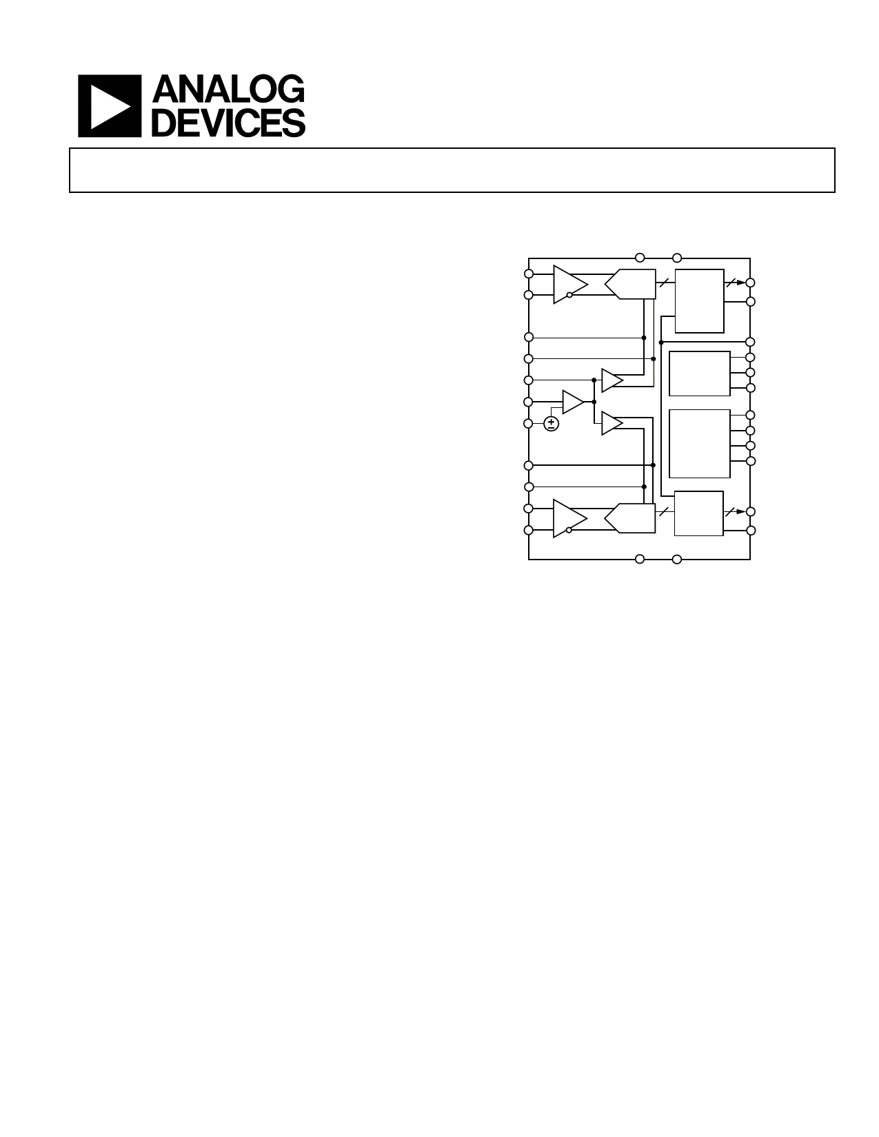
FUNCTIONAL BLOCK DIAGRAM
AVDD AGND
VIN+_A
VIN–_A
SHA
ADC
10 10
OUTPUT
MUX/
BUFFERS
D9_A–D0_A
OEB_A
REFT_A
REFB_A
VREF
SENSE
AGND
REFT_B
0.5V
CLOCK
DUTY CYCLE
STABILIZER
MODE
CONTROL
MUX_SELECT
CLK_A
CLK_B
DCS
SHARED_REF
PWDN_A
PWDN_B
DFS
REFB_B
VIN+_B
VIN–_B
SHA
AD9216
ADC
10 OUTPUT 10
MUX/
BUFFERS
D9_B–D0_B
OEB_B
DRVDD DRGND
Figure 1.
Fabricated on an advanced CMOS process, the AD9216 is avail-
able in a space saving, Pb-free, 64-lead LFCSP (9 mm × 9 mm) and
is specified over the industrial temperature range (−40°C to
+85°C).
PRODUCT HIGHLIGHTS
1. Pin compatible with AD9238, dual 12-bit 20 MSPS/40 MSPS/
65 MSPS ADC and AD9248, dual 14-bit 20 MSPS/40 MSPS/
65 MSPS ADC.
2. 105 MSPS capability allows for demanding, high frequency
applications.
3. Low power consumption: AD9216–105: 105 MSPS = 300 mW.
4. The patented SHA input maintains excellent performance for
input frequencies up to 200 MHz and can be configured for
single-ended or differential operation.
5. Typical channel crosstalk of < −80 dB at fIN up to 70 MHz.
6. The clock duty cycle stabilizer maintains performance over a
wide range of clock duty cycles.
One Technology Way, P.O. Box 9106, Norwood, MA 02062-9106, U.S.A.
Tel: 781.329.4700
www.analog.com
Fax: 781.461.3113 © 2005 Analog Devices, Inc. All rights reserved.
1 page 
AD9216
LOGIC SPECIFICATIONS
AVDD = 3.0 V, DRVDD = 2.5 V, maximum sample rate, CLK_A = CLK_B; AIN = −0.5 dBFS differential input, 1.0 V internal reference,
TMIN to TMAX, DCS enabled, unless otherwise noted.
Table 3.
Parameter
LOGIC INPUTS
High Level Input
Voltage
Low Level Input
Voltage
High Level Input
Current
Low Level Input
Current
Input Capacitance
LOGIC OUTPUTS1
DRVDD = 2.5 V
High Level Output
Voltage
Low Level Output
Voltage
Temp Test
Level
Full IV
Full IV
Full IV
Full IV
Full IV
Full IV
Full IV
AD9216BCPZ-65
Min Typ Max
2.0
−10
−10
2
0.8
+10
+10
2.45
0.05
AD9216BCPZ-80
Min Typ Max
AD9216BCPZ-105
Min Typ Max Unit
2.0
−10
−10
2
2.0 V
0.8 0.8 V
+10 −10
+10 µA
+10 −10
+10 µA
2 pF
2.45 2.45 V
0.05 0.05 V
1 Output voltage levels measured with 5 pF load on each output.
Rev. A | Page 5 of 40
5 Page 
TERMINOLOGY
Analog Bandwidth
The analog input frequency at which the spectral power of the
fundamental frequency (as determined by the FFT analysis) is
reduced by 3 dB.
Aperture Delay
The delay between the 50% point of the rising edge of the
encode command and the instant the analog input is sampled.
Aperture Uncertainty (Jitter)
The sample-to-sample variation in aperture delay.
Clock Pulse Width/Duty Cycle
Pulse-width high is the minimum amount of time that the
clock pulse should be left in a Logic 1 state to achieve rated
performance; pulse-width low is the minimum time clock pulse
should be left in a low state. At a given clock rate, these
specifications define an acceptable clock duty cycle.
Crosstalk
Coupling onto one channel being driven by a low level (−40
dBFS) signal when the adjacent interfering channel is driven by
a full-scale signal.
Differential Analog Input Resistance, Differential Analog
Input Capacitance, and Differential Analog Input
Impedance
The real and complex impedances measured at each analog
input port. The resistance is measured statically and the
capacitance and differential input impedances are measured
with a network analyzer.
Differential Analog Input Voltage Range
The peak-to-peak differential voltage that must be applied to
the converter to generate a full-scale response. Peak differential
voltage is computed by observing the voltage on a single pin
and subtracting the voltage from the other pin, which is 180°
out of phase. Peak-to-peak differential is computed by rotating
the inputs phase 180° and by taking the peak measurement
again. The difference is then computed between both peak
measurements.
Differential Nonlinearity
The deviation of any code width from an ideal 1 LSB step.
AD9216
Effective Number of Bits (ENOB)
The ENOB is calculated from the measured SINAD based on
the equation (assuming full-scale input)
ENOB
=
SINADMEASURED
6.02
− 1.76
dB
Full-Scale Input Power
Expressed in dBm and computed using the following equation.
⎜⎛ V 2 FULL SCALE rms ⎟⎞
⎜
PowerFULL SCALE = 10 log ⎜
⎜
Z INPUT
0.001
⎟
⎟
⎟
⎜⎝ ⎟⎠
Gain Error
The difference between the measured and ideal full-scale input
voltage range of the ADC.
Harmonic Distortion, Second
The ratio of the rms signal amplitude to the rms value of the
second harmonic component, reported in dBc.
Harmonic Distortion, Third
The ratio of the rms signal amplitude to the rms value of the
third harmonic component, reported in dBc.
Integral Nonlinearity
The deviation of the transfer function from a reference line
measured in fractions of 1 LSB using a best straight line
determined by a least square curve fit.
Minimum Conversion Rate
The encode rate at which the SNR of the lowest analog signal
frequency drops by no more than 3 dB below the guaran-
teed limit.
Maximum Conversion Rate
The encode rate at which parametric testing is performed.
Output Propagation Delay
The delay between a 50% crossing of the CLK rising edge and
the time when all output data bits are within valid logic levels.
Rev. A | Page 11 of 40
11 Page | ||
| Páginas | Total 30 Páginas | |
| PDF Descargar | [ Datasheet AD9216.PDF ] | |
Hoja de datos destacado
| Número de pieza | Descripción | Fabricantes |
| AD9211 | 1.8 V Analog-to-Digital Converter | Analog Devices |
| AD9212 | Serial LVDS A/D Converter | Analog Devices |
| AD9214 | 3V A/D Converter | Analog Devices |
| AD9215 | 3V A/D Converter | Analog Devices |
| Número de pieza | Descripción | Fabricantes |
| SLA6805M | High Voltage 3 phase Motor Driver IC. |
Sanken |
| SDC1742 | 12- and 14-Bit Hybrid Synchro / Resolver-to-Digital Converters. |
Analog Devices |
|
DataSheet.es es una pagina web que funciona como un repositorio de manuales o hoja de datos de muchos de los productos más populares, |
| DataSheet.es | 2020 | Privacy Policy | Contacto | Buscar |