|
|
|
PDF FAN102 Data sheet ( Hoja de datos )
| Número de pieza | FAN102 | |
| Descripción | Primary-Side-Control PWM Controller | |
| Fabricantes | Fairchild Semiconductor | |
| Logotipo | ||
Hay una vista previa y un enlace de descarga de FAN102 (archivo pdf) en la parte inferior de esta página. Total 14 Páginas | ||
|
No Preview Available !
August 2008
FAN102
Primary-Side-Control PWM Controller
Features
Constant-Voltage (CV) and Constant-Current (CC)
Control without Secondary-Feedback Circuitry
Green Mode: PWM Frequency Linearly Decreasing
Fixed PWM Frequency at 42kHz with Frequency
Hopping to Solve EMI Problem
Cable Compensation in CV Mode
Low Startup Current: 10μA
Low Operating Current: 3.5mA
Peak-Current-Mode Control in CV Mode
Cycle-by-Cycle Current Limiting
VDD Over-Voltage Protection with Auto-Restart
VDD Under-Voltage Lockout (UVLO)
Gate Output Maximum Voltage Clamped at 18V
Fixed Over-temperature Protection with Latch
SOP-8 Package Available
www.DataShAeept4pUl.iccomations
Battery chargers for cellular phones, cordless
phones, PDA, digital cameras, power tools
Replaces linear transformer and RCC SMPS
Description
This highly integrated PWM controller, FAN102,
provides several features to enhance the performance
of low-power flyback converters. The proprietary
topology enables simplified circuit design for battery
charger applications. A low-cost, smaller and lighter
charger results when compared to a conventional
design or a linear transformer. The startup current is
only 10µA, which allows use of large startup resistance
for further power saving.
To minimize the standby power consumption, the
proprietary green-mode function provides off-time
modulation to linearly decrease PWM frequency under
light-load conditions. This green-mode function assists
the power supply in meeting the power conservation
requirements.
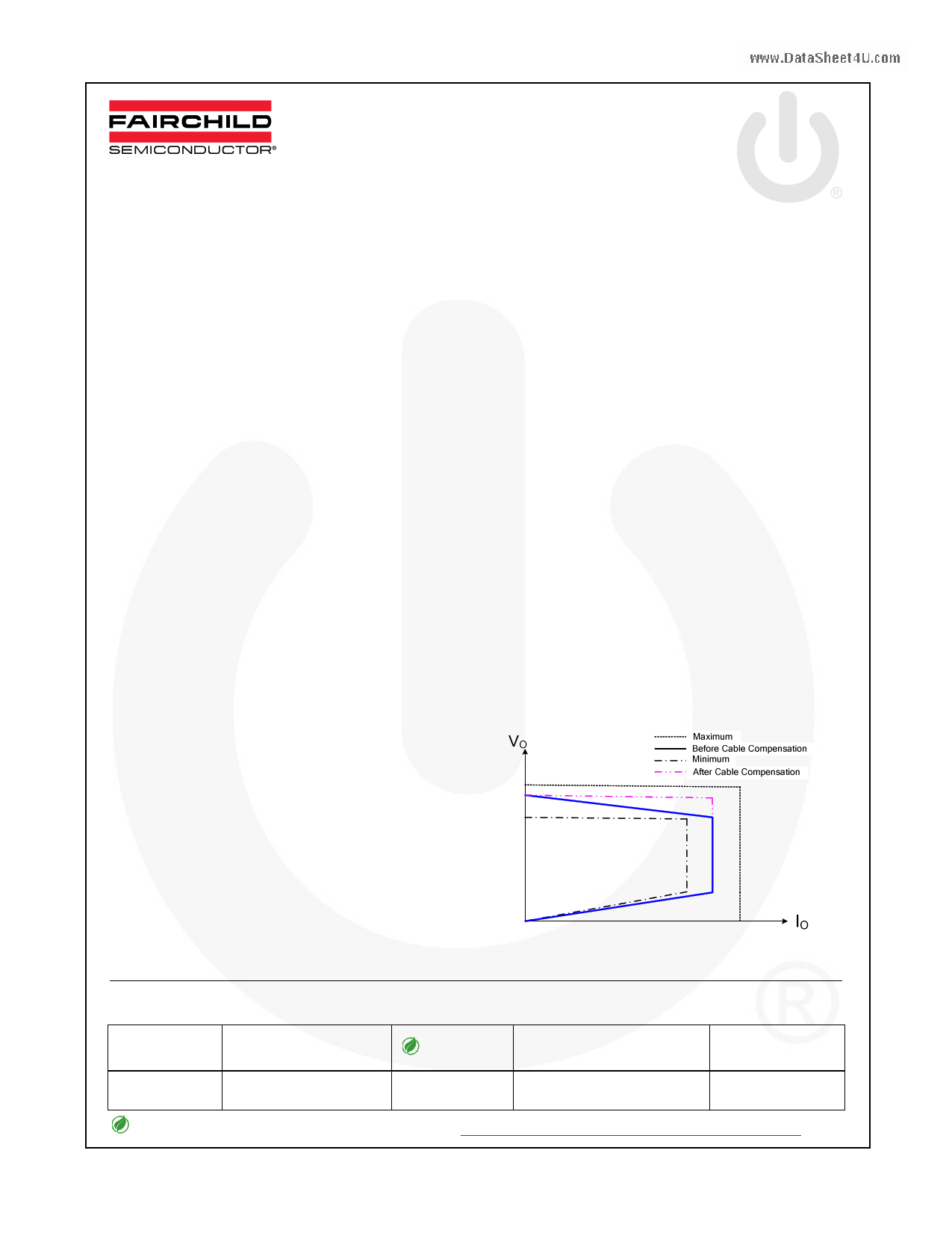
Using FAN102, a charger can be implemented with
fewer external components and minimized cost. A
typical output CV/CC characteristic envelope is shown
in Figure 1.
FAN102 controller is available in 8-pin SOP package.
Figure 1. Typical Output V-I Characteristic
Ordering Information
Part Number
Operating
Temperature Range
FAN102MY
-40°C to +105°C
Eco Status
Green
Package
8-Lead, Small Outline
Package (SOP-8)
Packing Method
Tape & Reel
For Fairchild’s definition of “green” Eco Status, please visit: http://www.fairchildsemi.com/company/green/rohs_green.html.
© 2008 Fairchild Semiconductor Corporation
FAN102 Rev. 1.0.1
www.fairchildsemi.com
1 page 
Electrical Characteristics
VDD=15V and TA=25°C unless otherwise specified.
Symbol
Parameter
Conditions
VDD Section
VOP Continuously Operating Voltage
VDD-ON Turn-On Threshold Voltage
VDD-OFF Turn-Off Threshold Voltage
IDD-OP
Operating Current
IDD-GREEN
Green-Mode Operating Supply
Current
VDD-OVP
tD-VDDOVP
VDD Over-Voltage Protection
Level
VDD Over-Voltage Protection
Debounce Time
VDD=20V, fS=fOSC,
VVS=2V,
VCS=3V, CL=1nF
VDD=20V, VVS=2.7V
fS=fOSC-N-MIN, VCS=0V
CL=1nF, VCOMV=0V
VCS=3V, VVS=2.3V
fs=fOSC, VVS=2.3V
Oscillator Section
Center Frequency
fOSC Frequency Frequency
Hopping Range
tFHR
fOSC-N-MIN
Frequency Hopping Period
Minimum Frequency at No Load
fOSC-CM-MIN Minimum Frequency at CCM
fDV
Frequency Variation vs. VDD
Deviation
fDT
Frequency Variation vs.
Temperature Deviation
TA=25°C
TA=25°C
TA=25°C
VVS=2.7V, VCOMV=0V
VVS=2.3V, VCS=0.5V
VDD=10V to 25V
TA=-40°C to +85°C
Voltage-Sense Section
www.DataSheetI4VUS-.UcVoPm
Sink Current for Brownout
Protection
Itc
VBIAS-COMV
IC Compensation Bias Current
Adaptive Bias Voltage
Dominated by VCOMV
Current-Sense Section
tPD
Propagation Delay to GATE
Output
tMIN-N
Minimum On Time at No Load
tMINCC
DSAW
VTH
Minimum On Time in CC Mode
Duty Cycle of SAW Limiter
Threshold Voltage for Current
Limit
RVS=20KΩ
VCOMV=0V, TA=25°C,
RVS=20KΩ
VVS=-0.8V, RS=2KΩ,
VCOMV=1V
VVS=0V, VCOMV=2V
Min.
15
4.5
27
100
39
±1.8
Typ. Max. Units
25
16 17
5.0 5.5
3.5 5.0
V
V
V
mA
12
28 29
250 400
mA
V
μs
42 45
±2.6 ±3.6
3
550
20
5
15
KHz
ms
Hz
KHz
%
%
125 μA
9.5 μA
1.4 V
100 200
ns
1100
400
40
1.3
ns
ns
%
V
Continued on the following page…
© 2008 Fairchild Semiconductor Corporation
FAN102 Rev. 1.0.1
5
www.fairchildsemi.com
5 Page 
Functional Description (Continued)
Under-Voltage Lockout (UVLO)
The turn-on and turn-off thresholds are fixed internally at
16V and 5V. During startup, the hold-up capacitor must
be charged to 16V through the startup resistor to enable
the FAN102. The hold-up capacitor continues to supply
VDD until power can be delivered from the auxiliary
winding of the main transformer. VDD must not drop
below 5V during this startup process. This UVLO
hysteresis window ensures that hold-up capacitor is
adequate to supply VDD during startup.
VDD Over-Voltage Protection (OVP)
VDD over-voltage protection prevents damage due to
over-voltage conditions. When the VDD voltage exceeds
28V due to abnormal conditions, PWM pulses are
disabled until the VDD voltage drops below the UVLO,
then start again. Over-voltage conditions are usually
caused by open feedback loops.
Over-Temperature Protection (OTP)
The built-in temperature-sensing circuit shuts down
PWM output once the junction temperature exceeds
140°C. While PWM output is shut down, the VDD voltage
gradually drops to the UVLO voltage. Some of the
FAN102’s internal circuits are shut down and VDD
gradually starts increasing again. When VDD reaches
16V, all the internal circuits, including the temperature-
sensing circuit, start operating normally. If the junction
temperature is still higher than 140°C, the PWM
controller shuts down immediately. This situation
continues until the temperature drops below 110°C.
Gate Output
The BiCMOS output stage is a fast totem-pole gate
driver. Cross conduction has been avoided to minimize
heat dissipation, increase efficiency, and enhance
reliability. The output driver is clamped by an internal
15V Zener diode to protect power MOSFET transistors
against undesired over-voltage gate signals.
Built-in Slope Compensation
The sensed voltage across the current-sense resistor is
used for current-mode control and pulse-by-pulse
current limiting. Built-in slope compensation improves
stability and prevents sub-harmonic oscillations due to
peak-current mode control. The FAN102 has a
synchronized, positively-sloped ramp built-in at each
switching cycle.
Noise Immunity
Noise from the current sense or the control signal can
cause significant pulse-width jitter, particularly in
continuous-conduction mode. While slope
compensation helps alleviate these problems, further
precautions should still be taken. Good placement and
layout practices should be followed. Avoiding long PCB
traces and component leads, locating compensation
and filter components near the FAN102, and increasing
the power MOS gate resistance are advised.
www.DataSheet4U.com
© 2008 Fairchild Semiconductor Corporation
FAN102 Rev. 1.0.1
11
www.fairchildsemi.com
11 Page | ||
| Páginas | Total 14 Páginas | |
| PDF Descargar | [ Datasheet FAN102.PDF ] | |
Hoja de datos destacado
| Número de pieza | Descripción | Fabricantes |
| FAN100 | Primary-Side-Control PWM Controller | Fairchild Semiconductor |
| FAN102 | Primary-Side-Control PWM Controller | Fairchild Semiconductor |
| FAN103 | Primary-Side-Regulation PWM Controller | Fairchild Semiconductor |
| FAN104 | Case Fan 120x120 | LogiLink |
| Número de pieza | Descripción | Fabricantes |
| SLA6805M | High Voltage 3 phase Motor Driver IC. |
Sanken |
| SDC1742 | 12- and 14-Bit Hybrid Synchro / Resolver-to-Digital Converters. |
Analog Devices |
|
DataSheet.es es una pagina web que funciona como un repositorio de manuales o hoja de datos de muchos de los productos más populares, |
| DataSheet.es | 2020 | Privacy Policy | Contacto | Buscar |