|
|
|
PDF MC34065-L Data sheet ( Hoja de datos )
| Número de pieza | MC34065-L | |
| Descripción | (MC3x065-x) High Performance Dual Channel Current Mode Controllers | |
| Fabricantes | ON Semiconductor | |
| Logotipo | ||
Hay una vista previa y un enlace de descarga de MC34065-L (archivo pdf) en la parte inferior de esta página. Total 18 Páginas | ||
|
No Preview Available !
www.DataSheet4U.com
MC34065−H, L
MC33065−H, L
High Performance
Dual Channel Current
Mode Controllers
The MC34065−H,L series are high performance, fixed frequency,
dual current mode controllers. They are specifically designed for
off−line and dc−to−dc converter applications offering the designer a
cost effective solution with minimal external components. These
integrated circuits feature a unique oscillator for precise duty cycle
limit and frequency control, a temperature compensated reference,
two high gain error amplifiers, two current sensing comparators, Drive
Output 2 Enable pin, and two high current totem pole outputs ideally
suited for driving power MOSFETs.
Also included are protective features consisting of input and
reference undervoltage lockouts each with hysteresis, cycle−by−cycle
current limiting, and a latch for single pulse metering of each output.
These devices are available in dual−in−line and surface mount
packages.
The MC34065−H has UVLO thresholds of 14 V (on) and 10 V (off),
ideally suited for off−line converters. The MC34065−L is tailored for
lower voltage applications having UVLO thresholds of 8.4 V (on) and
7.8 V (off).
• Unique Oscillator for Precise Duty Cycle Limit and Frequency Control
• Current Mode Operation to 500 kHz
• Automatic Feed Forward Compensation
• Separate Latching PWMs for Cycle−By−Cycle Current Limiting
• Internally Trimmed Reference with Undervoltage Lockout
• Drive Output 2 Enable Pin
• Two High Current Totem Pole Outputs
• Input Undervoltage Lockout with Hysteresis
• Low Startup and Operating Current
VCC 16
Vref
1
5
1
Sync Input
3
RT
CT
2
Voltage
Feedback 1
4
Compensation 1
5
5.0V
Reference
R
R
Vref
Undervoltage
Lockout
Oscillator
+
−
Error
Amp 1
VCC
Undervoltage
Lockout
Latching
PWM 1
Drive Output 1
7
Current Sense
61
Drive Output
2
Enable
14
Voltage
Feedback 2 13
Compensation 2
12
+
−
Error
Amp 2
Latching
PWM 2
Gnd 8
Drive Gnd 9
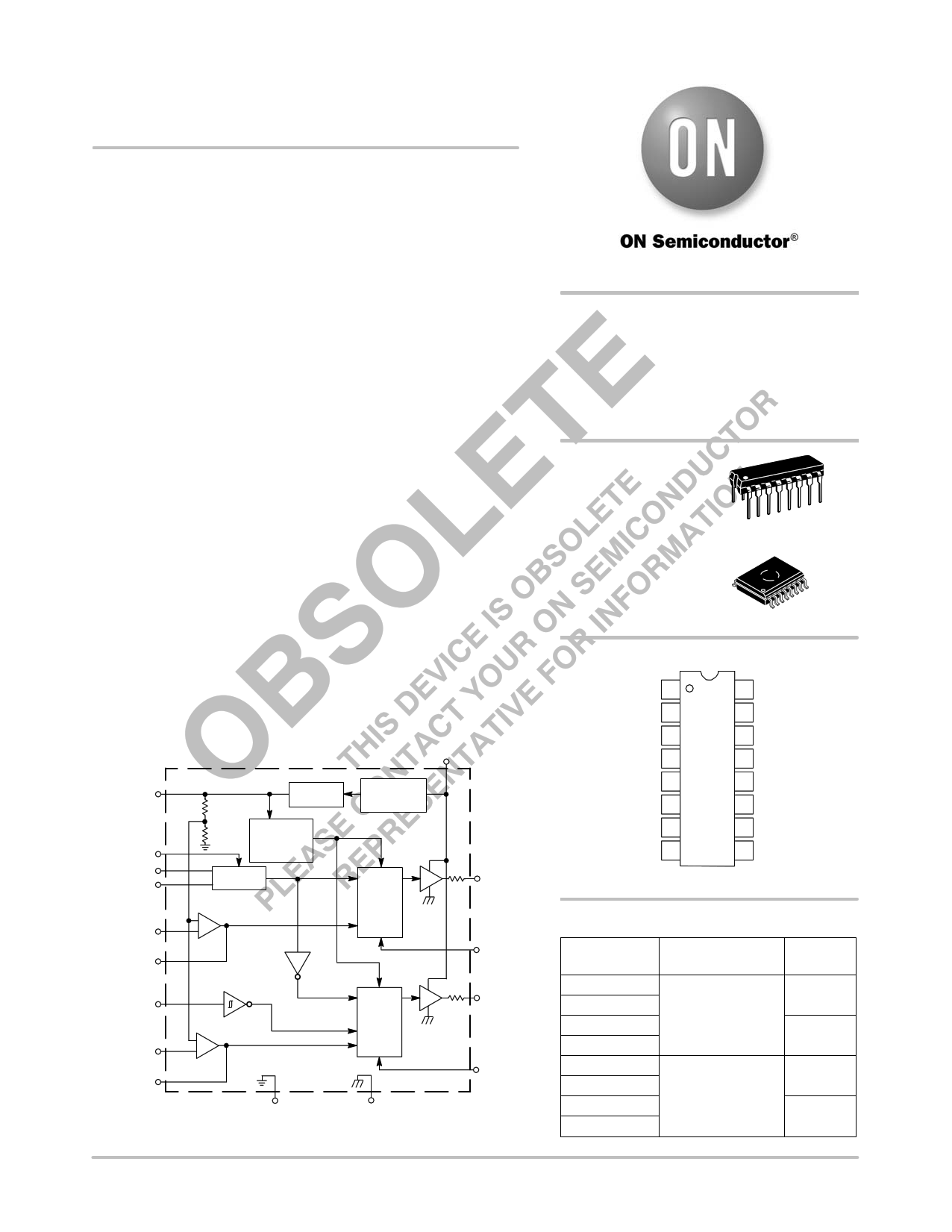
Representative Block Diagram
Drive Output 2
10
Current Sense
11 2
http://onsemi.com
HIGH PERFORMANCE
DUAL CHANNEL CURRENT
MODE CONTROLLERS
SEMICONDUCTOR
TECHNICAL DATA
P SUFFIX
PLASTIC PACKAGE
CASE 648
16
1
DW SUFFIX
PLASTIC PACKAGE
CASE 751G
(SO−16L)
16
1
PIN CONNECTIONS
Sync Input 1
CT 2
RT 3
Voltage Feedback 1 4
Compensation 1 5
Current Sense 1 6
Drive Output 1 7
16 VCC
15 Vref
14 Drive Output 2 Enable
13 Voltage Feedback
2
12 Compensation
2
11 Current Sense
2
10 Drive Output 2
Gnd 8
(Top View)
9 Drive
Gnd
ORDERING INFORMATION
Device
Operating
Temperature Range Package
MC34065DW−H
SO−16L
MC34065DW−L
MC34065P−H
TA = 0° to +70°C
Plastic DIP
MC34065P−L
MC33065DW−H
MC33065DW−L
MC33065P−H
MC33065P−L
TA = −40° to +85°C
SO−16L
Plastic DIP
© Semiconductor Components Industries, LLC, 2006
July, 2006 − Rev. 2
1
Publication Order Number:
MC34065−H/D
1 page 
MC34065−H, L
16
14 3.3 nF
12
500 pF
1.0 nF
100 pF
220 pF
10
5.0 nF
330 pF
8.0 2.2 nF
CT =
6.0 10 nF
VCC = 15 V
4.0 TA = 25°C
10 k 30 k 50 k 100 k
300 k 500 k 1.0 M
fOSC, OSCILLATOR FREQUENCY (Hz)
Figure 1. Timing Resistor versus
Oscillator Frequency
50
48
46 Output 2
44
42 VCC = 15 V
RT = 4.0 k to 16 k
TA = 25°
40 CL = 15 pF
Output 1
38
10 k
30 k 50 k 100 k
300 k 500 k
fOSC, OSCILLATOR FREQUENCY (Hz)
Figure 2. Maximum Output Duty Cycle
versus Oscillator Frequency
1.0 M
http://onsemi.com
5
5 Page 
MC34065−H, L
Sync
Input
Capacitor CT
Latch 1
Set" Input
Compensation
1
Current Sense
1
Latch 1
Reset" Input
Drive Output 1
Drive Output
2
Enable
Latch 2
Set" Input
Compensation
2
Current Sense
2
Latch 2
Reset" Input
Drive Output 2
Figure 16. Timing
Diagram
The outputs do not contain internal current limiting,
therefore an external series resistor may be required to
prevent the peak output current from exceeding the ±400
mA maximum rating. The sink saturation (VOL) is less than
0.75 V at 50 mA.
A separate Drive Ground pin is provided and, with proper
implementation, will significantly reduce the level of
switching transient noise imposed on the control circuitry.
This becomes particularly useful when reducing the Ipk(max)
clamp level. Figure 23 shows the proper ground connections
required for current sensing power MOSFET applications.
Drive Output 2 Enable Pin
This input is used to enable Drive Output 2. Drive
Output 1 can be used to control circuitry that must run
continuously such as volatile memory and the system clock,
or a remote controlled receiver, while Drive Output 2
controls the high power circuitry that is occasionally turned
off.
Reference
The 5.0 V bandgap reference is trimmed to ±2.0%
tolerance at TJ = 25°C. The reference has short circuit
protection and is capable of providing in excess of 30 mA for
powering any additional control system circuitry.
Design Considerations
Do not attempt to construct the converter on
wire−wrap or plug−in prototype boards. High frequency
circuit layout techniques are imperative to prevent
pulse−width jitter. This is usually caused by excessive noise
pick−up imposed on the Current Sense or Voltage Feedback
inputs. Noise immunity can be improved by lowering circuit
impedances at these points. The printed circuit layout should
contain a ground plane with low current signal and high
current switch and output grounds returning on separate
paths back to the input filter capacitor. Ceramic bypass
capacitors (0.1 μF) connected directly to VCC and Vref may
be required depending upon circuit layout. This provides a
low impedance path for filtering the high frequency noise.
All high current loops should be kept as short as possible
using heavy copper runs to minimize radiated EMI. The
Error Amp compensation circuitry and the converter output
voltage−divider should be located close to the IC and as far
as possible from the power switch and other noise generating
components.
http://onsemi.com
11
11 Page | ||
| Páginas | Total 18 Páginas | |
| PDF Descargar | [ Datasheet MC34065-L.PDF ] | |
Hoja de datos destacado
| Número de pieza | Descripción | Fabricantes |
| MC34065-H | (MC3x065-x) High Performance Dual Channel Current Mode Controllers | ON Semiconductor |
| MC34065-H | High Performance Dual Channel Current Mode Controllers | Motorola Semiconductors |
| MC34065-L | (MC3x065-x) High Performance Dual Channel Current Mode Controllers | ON Semiconductor |
| MC34065-L | High Performance Dual Channel Current Mode Controllers | Motorola Semiconductors |
| Número de pieza | Descripción | Fabricantes |
| SLA6805M | High Voltage 3 phase Motor Driver IC. |
Sanken |
| SDC1742 | 12- and 14-Bit Hybrid Synchro / Resolver-to-Digital Converters. |
Analog Devices |
|
DataSheet.es es una pagina web que funciona como un repositorio de manuales o hoja de datos de muchos de los productos más populares, |
| DataSheet.es | 2020 | Privacy Policy | Contacto | Buscar |