|
|
|
PDF MC33025 Data sheet ( Hoja de datos )
| Número de pieza | MC33025 | |
| Descripción | High Speed Double-Ended PWM Controller | |
| Fabricantes | Motorola Semiconductors | |
| Logotipo | ||
Hay una vista previa y un enlace de descarga de MC33025 (archivo pdf) en la parte inferior de esta página. Total 20 Páginas | ||
|
No Preview Available !
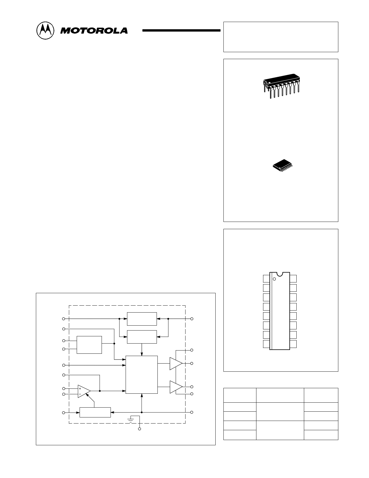
High Speed Double-Ended
PWM Controller
Order this document by MC34025/D
MC34025
MC33025
The MC34025 series are high speed, fixed frequency, double–ended
pulse width modulator controllers optimized for high frequency operation.
They are specifically designed for Off–Line and DC–to–DC converter
applications offering the designer a cost effective solution with minimal
external components. These integrated circuits feature an oscillator, a
temperature compensated reference, a wide bandwidth error amplifier, a
high speed current sensing comparator, steering flip–flop, and dual high
current totem pole outputs ideally suited for driving power MOSFETs.
Also included are protective features consisting of input and reference
undervoltage lockouts each with hysteresis, cycle–by–cycle current limiting,
and a latch for single pulse metering.
The flexibility of this series allows it to be easily configured for either
current mode or voltage mode control.
• 50 ns Propagation Delay to Outputs
• Dual High Current Totem Pole Outputs
• Wide Bandwidth Error Amplifier
• Fully–Latched Logic with Double Pulse Suppression
• Latching PWM for Cycle–By–Cycle Current Limiting
• Soft–Start Control with Latched Overcurrent Reset
• Input Undervoltage Lockout with Hysteresis
• Low Start–Up Current (500 µA Typ)
• Internally Trimmed Reference with Undervoltage Lockout
• 90% Maximum Duty Cycle (Externally Adjustable)
• Precision Trimmed Oscillator
• Voltage or Current Mode Operation to 1.0 MHz
• Functionally Similar to the UC3825
16
Vref
4
Clock
5
RT
CT
6
7
Ramp
Error Amp 3
Output
Noninverting 2
Input
Inverting
Input 1
8
Soft–Start
Simplified Application
Oscillator
5.1V
Reference
UVLO
Latching
PWM and
Error
Amp
Steering
Flip Flop
Soft–Star
t
10 Ground
This device contains 227 active transistors.
15
VCC
13
VC
14
Output B
11
Output A
Power
12 Ground
9
Current
Limit/
Shutdown
16
1
P SUFFIX
PLASTIC PACKAGE
CASE 648
16
1
DW SUFFIX
PLASTIC PACKAGE
CASE 751G
(SO–16L)
PIN CONNECTIONS
Error Amp
Inverting Input
Error Amp
Noninverting Input
Error Amp Output
1
2
3
16 Vref
15 VCC
14 Output B
Clock 4
RT 5
13 VC
12 Power Ground
CT 6
Ramp 7
Soft–Start 8
11 Output A
10 Ground
9 Current Limit/
Shutdown
(Top View)
ORDERING INFORMATION
Device
Operating
Temperature Range
Package
MC33025DW
SO–16L
TA = – 40° to +105°C
MC33025P
Plastic DIP
MC34025DW
MC34025P
TA = 0° to +70°C
SO–16L
Plastic DIP
MOTOROLA ANALOG IC DEVICE DATA
© Motorola, Inc. 1996
Rev 1
1
1 page 
MC34025 MC33025
Figure 7. Reference Voltage Change
versus Source Current
0
–5.0
VCC = 15 V
–10
–15
TA = – 55°C
TA = +125°C
TA = + 25°C
–20
–25
–30
0
10 20 30 40
ISource, SOURCE CURRENT (mA)
50
Figure 8. Reference Short Circuit Current
versus Temperature
66
65.6 VCC = 15 V
65.2
64.8
64.4
64
–55 – 25
0 25 50 75 100
TA, AMBIENT TEMPERATURE (°C)
125
Figure 9. Reference Line Regulation
Figure 10. Reference Load Regulation
Vref LINE REGULATION 10 V – 24 V
2.0 ms/DIV
Vref LINE REGULATION 1.0 mA – 10 mA
2.0 ms/DIV
Figure 11. Current Limit Comparator Threshold
Change versus Temperature
4.0
2.0
0
– 2.0
– 4.0
– 6.0
– 8.0
–10
–12
– 50 – 25 0 25 50 75 100 125
TA, AMBIENT TEMPERATURE (°C)
Figure 12. Shutdown Comparator Threshold
Voltage versus Temperature
1.50
1.46 VCC = 15 V
1.42
1.38
1.34
1.30
–55
–25 0 25 50 75 100
TA, AMBIENT TEMPERATURE (°C)
125
MOTOROLA ANALOG IC DEVICE DATA
5
5 Page 
MC34025 MC33025
Figure 23. Dead Time Addition
Vref
RDT 4
5
6
RT CT
Oscillator
Figure 24. External Clock Synchronization
5.0 V
0V
RT
4
5
6
CT
Oscillator
Additional dead time can be added by the addition of a dead time resistor from
Vref to CT. See text on oscillator section for more information.
The sync pulse fed into the clock pin must be at least 3.9 V. RT and CT need
to be set 10% slower than the sync frequency. This circuit is also used in voltage
mode operation for master/slave operation. The clock signal would be coming
from the master which is set at the desired operating frequency, while the slave
is set 10% slower.
Figure 25. Resistive Current Sensing
9 ISense
The addition of an RC filter will eliminate instability caused by the leading edge spike
on the current waveform. This sense signal can also be used at the ramp input pin for
current mode control. For ramp compensation it is necessary to know the gain of the
current feedback loop. If a transformer is used, the gain can be calculated by:
+ RSense
Ai turns ratio
Figure 26. Primary Side Current Sensing
Figure 27. Primary or Secondary Side
Current Sensing
9 Rw ISense
9
Rw
0
ISense
The addition of an RC filter will eliminate instability caused by the leading edge spike on the current waveform. This sense signal can also be used at the ramp input
pin for current mode control. For ramp compensation it is necessary to know the gain of the current feedback loop. The gain can be calculated by:
+Ai
Rw
turns ratio
MOTOROLA ANALOG IC DEVICE DATA
11
11 Page | ||
| Páginas | Total 20 Páginas | |
| PDF Descargar | [ Datasheet MC33025.PDF ] | |
Hoja de datos destacado
| Número de pieza | Descripción | Fabricantes |
| MC3302 | Quad voltage comparator | NXP Semiconductors |
| MC3302 | Quad Single Supply Comparators | Motorola Semiconductors |
| MC3302 | Single Supply Quad Comparators | ON Semiconductor |
| MC33023 | High Speed Single-Ended PWM Controller | Motorola Semiconductors |
| Número de pieza | Descripción | Fabricantes |
| SLA6805M | High Voltage 3 phase Motor Driver IC. |
Sanken |
| SDC1742 | 12- and 14-Bit Hybrid Synchro / Resolver-to-Digital Converters. |
Analog Devices |
|
DataSheet.es es una pagina web que funciona como un repositorio de manuales o hoja de datos de muchos de los productos más populares, |
| DataSheet.es | 2020 | Privacy Policy | Contacto | Buscar |