|
|
|
PDF NS486SXL Data sheet ( Hoja de datos )
| Número de pieza | NS486SXL | |
| Descripción | Optimized 32-Bit 486-Class Controller with On-Chip Peripherals for Embedded Systems | |
| Fabricantes | National | |
| Logotipo | ||
Hay una vista previa y un enlace de descarga de NS486SXL (archivo pdf) en la parte inferior de esta página. Total 26 Páginas | ||
|
No Preview Available !
ADVANCE INFORMATION
December 1997
NS486™SXL
Optimized 32-Bit 486-Class Controller with On-Chip
Peripherals for Embedded Systems
General Description
The NS486SXL is a highly integrated embedded system
controller incorporating an Intel486™-class 32-bit processor
along with all of the necessary System Service Elements,
implementing a true “system on a chip.” It is ideally suited for
a wide variety of applications running in a segmented
protect-mode environment. The NS486SXL is the second
member of the NS486 family.
Features
n 100% compatible with VxWorks™, VRTX™, QNX™
Neutrino, pSOS +®, and other popular real-time
executives and operating system kernels
n Intel486 instruction set compatible (protected mode only)
with optimized performance
n Operation at 25 MHz with 5V supply
n Low cost 132-pin PQFP package
n Industry standard interrupt controller, timers, and real
time clock
n Protected WATCHDOG™ timer
n Optimized DRAM Controller (supports two banks, up to
8 Mbytes each)
n Up to nine versatile, programmable chip selects
n Up to eight external interrupts directly supported, and
additional interrupt expansion through an external PIC
interface
n Glueless interface to ISA-type peripherals
n Arbitration support for auxiliary processor
n Support for External Bus Masters, allowing them to
access DRAM and on-chip Peripherals
n MICROWIRE™/Access.bus synchronous serial
interfaces
n UART with IrDA v1.0 (Infrared Data Association) port
n Reconfigurable I/O: Up to 28 I/O pins can be used as
general purpose bidirectional I/O lines
n Flexible, programmable, multilevel power saving modes
maximize power savings
n Programming model compatible with the NS486SXF
where possible
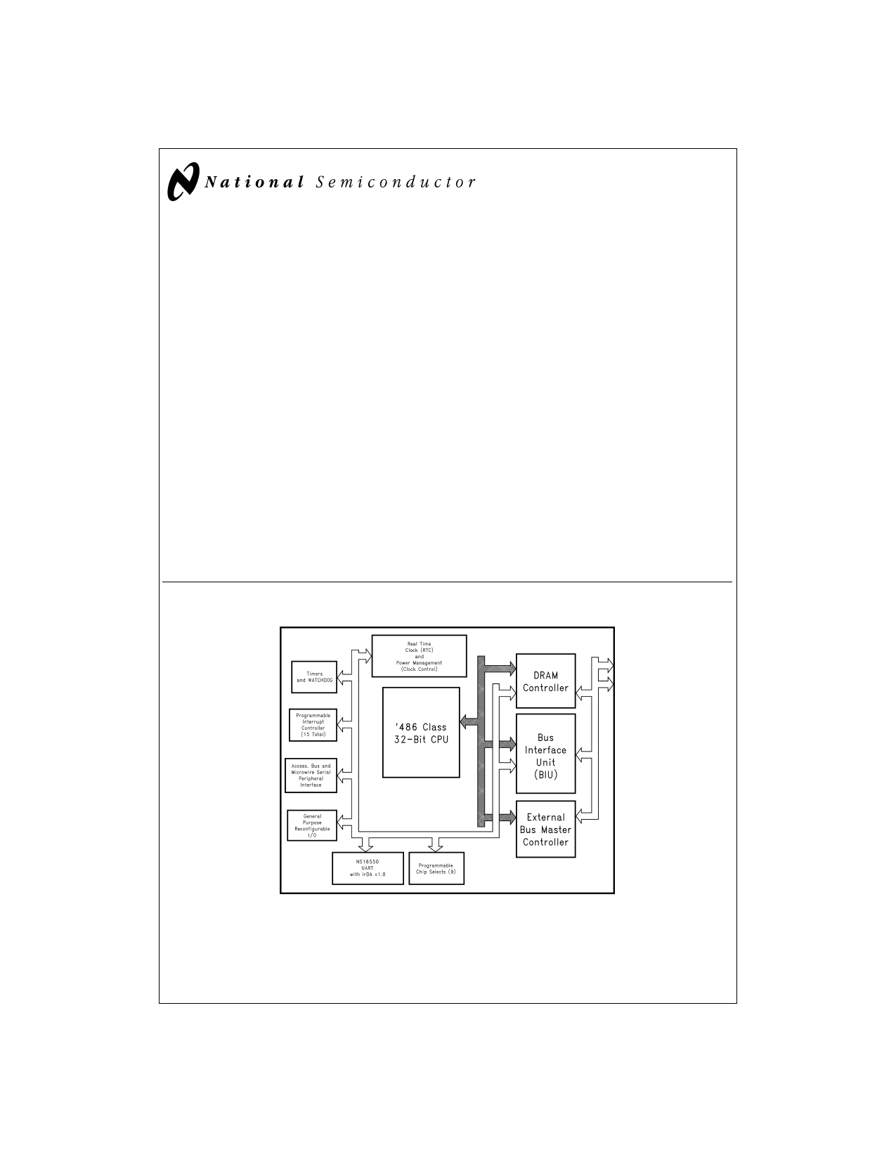
Block Diagram NS486SXL Single-Chip Embedded Controller
MICROWIRE™, NS486™ and WATCHDOG™ are trademarks of National Semiconductor Corporation.
TRI-STATE® is a registered trademark of National Semiconductor Corporation.
Intel486™ is a trademaek of Intel Corporation.
pSOS +™ is a trademark of Integrated Systems, Inc.
VRTX™ is a registered trademark of Microtec Research, Inc.
PowerPack® is a registered trademark of Microtek International.
QNX™ is a registered trademark of QNX Software Systems, Inc.
VxWorks™ is a registered trademark of Wind River Systems, Inc.
© 1998 National Semiconductor Corporation DS100121
DS100121-1
www.national.com
1 page 
1.0 System Overview (Continued)
1.3.6 Power Management Features
The NS486SXL power management structure includes a
number of power saving mechanisms that can be combined
to achieve comprehensive power savings under a variety of
system conditions. First of all, the core processor power con-
sumption can be controlled by varying the processor/system
clock frequency. The internal CPU clock can be divided by 4,
8, 16, 32 or 64. In addition, in idle mode, the internal proces-
sor clock will be disabled. Finally, if an external crystal oscil-
lator circuit is being used, it can be disabled. For maximum
power savings, all internal clocks can be disabled (except for
the real-time clock oscillator).
The clocks of the on-board peripherals can be individually or
globally controlled. By setting bits in the power management
control registers, the internal clocks to the three-wire inter-
face, the timer, the DRAM controller, and the UART can be
disabled.
In addition to these internal clocks, the external SYSCLK can
be disabled via a bit in the power management control regis-
ters.
Using various combinations of these power saving controls
with the NS486SXL controller will result in excellent pro-
grammable power management for any application.
1.4 NS486SXL SYSTEM BUS
The NS486SXL system bus provides the interface to off-chip
peripherals and memory. It offers an ISA compatible inter-
face and is therefore capable of directly interfacing to many
ISA peripheral control devices. The interface is accom-
plished through the Bus Interface Unit (BIU). The BIU gener-
ates all of the access signals for both internal and external
peripherals and memory. Depending upon whether the ac-
cess is to internal peripherals, external peripherals or exter-
nal memory, the BIU generates the timing and control sig-
nals to access those resources. The BIU is designed to
support a glueless interface to many ISA-type peripherals.
For debug purposes, the NS486SXL can be set to generate
external bus cycles at the same time as an internal periph-
eral access takes place. This gives logic analyzers or other
debug tools the ability to track and capture internal periph-
eral accesses.
FIGURE 2. NS486SXL Internal Busses
DS100121-3
Access to internal peripherals is accomplished in three CPU
T-states (clock cycles). The fastest access to off-chip I/O is
also three T-states. When accessing off-chip memory and
I/O, wait state generation is accomplished through a combi-
nation of NS486SXL chip select logic and off-chip peripheral
feedback signals.
The ISA-like bus on the NS486SXL also supports External
Bus Masters. This feature allows external processors or I/O
Peripherals (and customer proprietary ASICs) with built-in
DMA controllers to read and write System DRAM supported
by the ’SXL DRAM Controller. External Masters can also ac-
cess any internal or external peripherals or memory as well.
The external master address must be at TRI-STATE®
(through external address transceivers if necessary) in order
to support external master access to the DRAM.
5 www.national.com
5 Page 
2.0 SXL Pin Description Tables (Continued)
TABLE 7. Auxiliary Processor Interface Pins
Symbol
EREQ
EACK
DRV
Pins
52
53
54
Type
O
I
O
Function
External bus REQuest (active-low) to an auxiliary processor. This signal is
asserted whenever the auxiliary processor feature of a programmable chip select
is enabled. This is used to request access to a shared memory from another
processor.
External bus ACKnowledge (active-low) from an auxiliary processor.
Auxiliary processor shared memory DRiVe control signal. Once access is granted
to the shared memory, this signal is asserted to enable the address, data and
control signal buffers to drive the shared memory pins.
Symbol
TEST
Pins
42
TABLE 8. Test Pins
Type
I
Function
Reserved for testing and development system support. Normally pulled high. A
small number of test modes are documented for use by the customer. While
TEST is asserted, all output pins except OSCX2 and RTCX2 are TRI-STATE.
Symbol
NMI
INTA
IRQ[7:0]
Pins
55
56
46, 47, 57, 58,
59, 60, 61, 62
TABLE 9. Interrupt Control Pins
Type
I
O
I
Function
Non-Maskable Interrupt. This active-high signal will generate a non-maskable
interrupt to the CPU when it is active high. Normally this signal is used to indicate
a serious system error.
INTerrupt Acknowledge. During each interrupt acknowledge cycle this signal will
strobe low; it should be used by external cascaded interrupt controllers.
Interrupt ReQuests. These inputs are either rising edge or low-level sensitive
interrupt requests, depending on the configuration of the internal interrupt
controllers. These interrupt requests may also be programmed to support
externally cascaded interrupt controller(s). The IRQ pins are also used to select a
particular test in test mode.
Symbol
RTCX1
RTCX2
Vbat
Pins
38
40
41
TABLE 10. Real Time Clock Pins
Type
I
O
I
Function
Real Time Clock crystal oscillator input: 32 kHz crystal.
Real Time Clock crystal oscillator output: 32 kHz crystal.
External + battery input for real time clock.
Symbol
SYSCLK
OSCX1
Pins
73
22
TABLE 11. Oscillator Pins
Type
O
I
Function
SYStem CLocK. This clock output pin will either be driven with a signal half the
frequency of the OSCX1 input clock frequency or the CPU’s clock frequency,
which is determined in the Power Management Control Register 1. The source
selection for this signal is determined by bit 1 of the Power Management Control
Register 3.
OSCillator Crystal 1 input. This pin should either be driven by a TTL oscillator or
be connected to an external crystal circuit. This signal is the fundamental clock
source for all clocked elements in the NS486SXL, except the Real-Time Clock,
which has its own crystal pins.
11 www.national.com
11 Page | ||
| Páginas | Total 26 Páginas | |
| PDF Descargar | [ Datasheet NS486SXL.PDF ] | |
Hoja de datos destacado
| Número de pieza | Descripción | Fabricantes |
| NS486SXF | NS486 SXF Optimized 32-Bit 486-Class Cntrll w/On-Chip Peri for Embedded Sys (Rev. A) | Texas Instruments |
| NS486SXF | NS486TMSXF Optimized 32-Bit 486-Class Controller with On-Chip Peripherals for Embedded Systems | National |
| NS486SXL | Optimized 32-Bit 486-Class Controller with On-Chip Peripherals for Embedded Systems | National |
| NS486SXLVUL | Optimized 32-Bit 486-Class Controller with On-Chip Peripherals for Embedded Systems | National Semiconductor |
| Número de pieza | Descripción | Fabricantes |
| SLA6805M | High Voltage 3 phase Motor Driver IC. |
Sanken |
| SDC1742 | 12- and 14-Bit Hybrid Synchro / Resolver-to-Digital Converters. |
Analog Devices |
|
DataSheet.es es una pagina web que funciona como un repositorio de manuales o hoja de datos de muchos de los productos más populares, |
| DataSheet.es | 2020 | Privacy Policy | Contacto | Buscar |