|
|
|
PDF MAX4517 Data sheet ( Hoja de datos )
| Número de pieza | MAX4517 | |
| Descripción | Dual-Supply / Low-On-Resistance / SPST / CMOS Analog Switches | |
| Fabricantes | Maxim Integrated | |
| Logotipo | ||
Hay una vista previa y un enlace de descarga de MAX4517 (archivo pdf) en la parte inferior de esta página. Total 8 Páginas | ||
|
No Preview Available !
19-1068; Rev 0; 6/96
Dual-Supply, Low-On-Resistance,
SPST, CMOS Analog Switches
_______________General Description
The MAX4516/MAX4517 are single-pole/single-throw
(SPST), CMOS, low-voltage, dual-supply analog switch-
es with very low switch on-resistance. The MAX4516 is
normally open (NO). The MAX4517 is normally closed
(NC).
These CMOS switches can operate continuously with
dual supplies between ±1V and ±6V. Each switch can
handle rail-to-rail analog signals. The off-leakage cur-
rent maximum is only 1nA at +25°C or 20nA at +85°C.
The digital input is referenced to the positive power
supply and is CMOS compatible.
For pin-compatible parts for use with a single supply,
refer to the MAX4514/MAX415.
________________________Applications
Battery-Operated Equipment
Audio and Video Signal Routing
Low-Voltage Data-Acquisition Systems
Communications Circuits
PCMCIA Cards
Cellular Phones
Modems
____________________________Features
o Available in SOT23-5 Package
o ±1V to ±6V Dual-Supply Operation
o Guaranteed On-Resistance: 20Ω with ±5V
Supplies
o Guaranteed Low Off-Leakage Currents:
1nA at +25°C
20nA at +85°C
o Guaranteed Low On-Leakage Currents:
2nA at +25°C
40nA at +85°C
o Low Charge Injection: 20pC Max
o Fast Switching Speed: tON = 100ns, tOFF = 75ns
o tON > tOFF at ±5V
o CMOS Logic Compatible with ±5V Supplies
______________Ordering Information
PART
MAX4516CPA
MAX4516CSA
MAX4516CUK
MAX4516C/D
TEMP. RANGE
0°C to +70°C
0°C to +70°C
0°C to +70°C
0°C to +70°C
PIN-PACKAGE
8 Plastic DIP
8 SO
5 SOT23-5
Dice*
Ordering Information continued at end of data sheet.
*Contact factory for dice specifications.
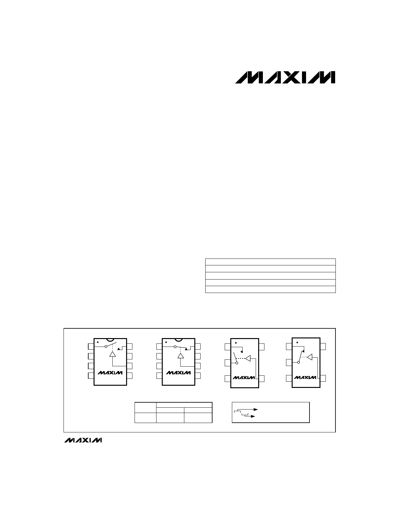
__________________________________________________________Pin Configurations
TOP VIEW
COM 1
N.C. 2
N.C. 3
V+ 4
MAX4516
DIP/SO
8 NO COM 1
7 V-
N.C. 2
6 IN
N.C. 3
5 N.C.
V+ 4
MAX4517
DIP/SO
8 NC COM 1
5 V+ COM 1
5 V+
7 V-
6 IN
NO 2
NC 2
5 N.C.
V- 3
4 IN
MAX4516
V- 3
4 IN
MAX4517
SOT23-5
SOT23-5
N.C. = NOT INTERNALLY CONNECTED
INPUT
LOW
HIGH
SWITCH STATE
MAX4516
MAX4517
OFF ON
ON OFF
MARKING INFORMATION (SOTs only)
XX XX
LOT SPECIFIC CODE
AG = MAX4516
AH = MAX4517
________________________________________________________________ Maxim Integrated Products 1
For free samples & the latest literature: http://www.maxim-ic.com, or phone 1-800-998-8800
http://www.Datasheet4U.com
1 page 
Dual-Supply, Low-On-Resistance,
SPST, CMOS Analog Switches
______________________________________________________________Pin Description
MAX4517PIN
MAX4516
MAX4517
NAME
FUNCTION
DIP/SO
1
2, 3, 5
4
6
7
8
—
SOT23-5
1
—
5
4
3
2
—
DIP/SO
1
2, 3, 5
4
6
7
—
8
SOT23-5
1
—
5
4
3
—
2
COM
N.C.
V+
IN
V-
NO
NC
Analog Switch Common Terminal
No Connect (not internally connected)
Positive Supply-Voltage Input (analog and digital)
Digital Control Input
Negative Supply-Voltage Input (analog and digital)
Analog Switch (normally open)
Analog Switch (normally closed)
Note: NO, NC, and COM pins are identical and interchangeable. Any may be considered as an input or an output; signals pass
equally well in both directions.
__________Applications Information
Power-Supply Considerations
The MAX4516/MAX4517 operate with power-supply
voltages from ±1V to ±6V, but are tested and guaran-
teed only with ±5V supplies. Similarly, they will operate
with a single +2V to +12V supply, but logic-level inputs
can shift with higher voltages. The pin-compatible
MAX4514/MAX4515 are recommended for use with a
single supply.
The MAX4516/MAX4517 construction is typical of most
CMOS analog switches, except that they have only two
supply pins: V+ and V-. V+ and V- drive the internal
CMOS switches and set their analog voltage limits.
Reverse ESD-protection diodes are internally connected
between each analog-signal pin and both V+ and V-.
One of these diodes conducts if any analog signal
exceeds V+ or V-.
Virtually all the analog leakage current comes from the
ESD diodes to V+ or V-. Although the ESD diodes on a
given signal pin are identical and therefore fairly well
balanced, they are reverse biased differently. Each is
biased by either V+ or V- and the analog signal. This
means their leakages will vary as the signal varies. The
difference in the two diode leakages to the V+ and V-
pins constitutes the analog-signal-path leakage current.
All analog leakage current flows between each pin and
one of the supply terminals, not to the other switch ter-
minal. This is why both sides of a given switch can
show leakage currents of the same or opposite polarity.
There is no connection between the analog-signal
paths and V+ or V-.
V+ and V- also power the internal logic and logic-level
translators. The logic-level translators convert the logic
levels to switched V+ and V- signals to drive the analog
signal gates.
Logic-Level Thresholds
The logic-level thresholds are CMOS-compatible but
not TTL-compatible. Since these parts have no
ground pin, the logic-level threshold is referenced to
V+. The threshold limits are V+ = -1.5V and V+ = -3.5V
for V+ levels between +6V and +3V. When V+ = +2V,
the logic threshold is approximately 0.6V.
Do not connect the MAX4516/MAX4517’s V+ to +3V
and then connect the logic-level pins to logic-level
signals that operate from a +5V supply. TTL levels
can exceed +3V and violate the absolute maximum
ratings, damaging the part and/or external circuits.
High-Frequency Performance
In 50Ω systems, signal response is reasonably flat up
to 250MHz (see Typical Operating Characteristics).
Above 20MHz, the on response has several minor
peaks that are highly layout dependent. The problem is
not in turning the switch on; it’s in turning it off. The off-
state switch acts like a capacitor and passes higher fre-
quencies with less attenuation. At 10MHz, off isolation is
about -48dB in 50Ω systems, decreasing (approximate-
ly 20dB per decade) as frequency increases. Higher cir-
cuit impedances also cause off isolation to decrease.
Off isolation is about 3dB above that of a bare IC sock-
et, and is due entirely to capacitive coupling.
_______________________________________________________________________________________ 5
http://www.Datasheet4U.com
5 Page | ||
| Páginas | Total 8 Páginas | |
| PDF Descargar | [ Datasheet MAX4517.PDF ] | |
Hoja de datos destacado
| Número de pieza | Descripción | Fabricantes |
| MAX451 | CMOS Video Amplifier | Maxim Integrated |
| MAX4510 | Rail-to-Rail / Fault-Protected / SPST Analog Switches | Maxim Integrated |
| MAX4511 | Quad / Rail-to-Rail / Fault-Protected / SPST Analog Switches | Maxim Integrated |
| MAX4512 | Quad / Rail-to-Rail / Fault-Protected / SPST Analog Switches | Maxim Integrated |
| Número de pieza | Descripción | Fabricantes |
| SLA6805M | High Voltage 3 phase Motor Driver IC. |
Sanken |
| SDC1742 | 12- and 14-Bit Hybrid Synchro / Resolver-to-Digital Converters. |
Analog Devices |
|
DataSheet.es es una pagina web que funciona como un repositorio de manuales o hoja de datos de muchos de los productos más populares, |
| DataSheet.es | 2020 | Privacy Policy | Contacto | Buscar |