|
|
|
PDF TC1107 Data sheet ( Hoja de datos )
| Número de pieza | TC1107 | |
| Descripción | 300mA CMOS LDO with Shutdown and VREF Bypass | |
| Fabricantes | Microchip | |
| Logotipo | ||
Hay una vista previa y un enlace de descarga de TC1107 (archivo pdf) en la parte inferior de esta página. Total 12 Páginas | ||
|
No Preview Available !
TC1107
300mA CMOS LDO with Shutdown and VREF Bypass
Features
• Extremely Low Supply Current (50µA, Typ.)
• Very Low Dropout Voltage
• 300mA Output Current
• High Output Voltage Accuracy
• Standard or Custom Output Voltages
• Power Saving Shutdown Mode
• Bypass Input for Ultra Quiet Operation
• Over Current and Over Temperature Protection
• Space-Saving MSOP Package Option
Applications
• Battery Operated Systems
• Portable Computers
• Medical Instruments
• Instrumentation
• Cellular/GSM/PHS Phones
• Linear Post-Regulators for SMPS
• Pagers
Device Selection Table
Part Number
Package
Junction
Temp. Range
TC1107-xxVOA 8-Pin SOIC -40°C to +125°C
TC1107-xxVUA 8-Pin MSOP -40°C to +125°C
NOTE: xx indicates output voltages
Available Output Voltages: 2.5, 2.8, 3.0, 3.3, 5.0.
Other output voltages are available. Please contact Microchip
Technology Inc. for details.
Package Type
8-Pin MSOP
VOUT 1
8 VIN
GND 2 TC1107VUA 7 NC
NC 3
6 NC
Bypass 4
5 SHDN
General Description
The TC1107 is a fixed output, high accuracy (typically
±0.5%) CMOS upgrade for older (bipolar) low dropout
regulators. Total supply current is typically 50µA at full
load (20 to 60 times lower than in bipolar regulators).
TC1107 key features include ultra low noise operation
(plus optional Bypass input); very low dropout voltage
(typically 240mV at full load), and fast response to step
changes in load. Supply current is reduced to 0.05µA
(typical) and VOUT falls to zero when the shutdown
input is low.
The TC1107 incorporates both over temperature and
over current protection. The TC1107 is stable with an
output capacitor of only 1µF and has a maximum
output current of 300mA.
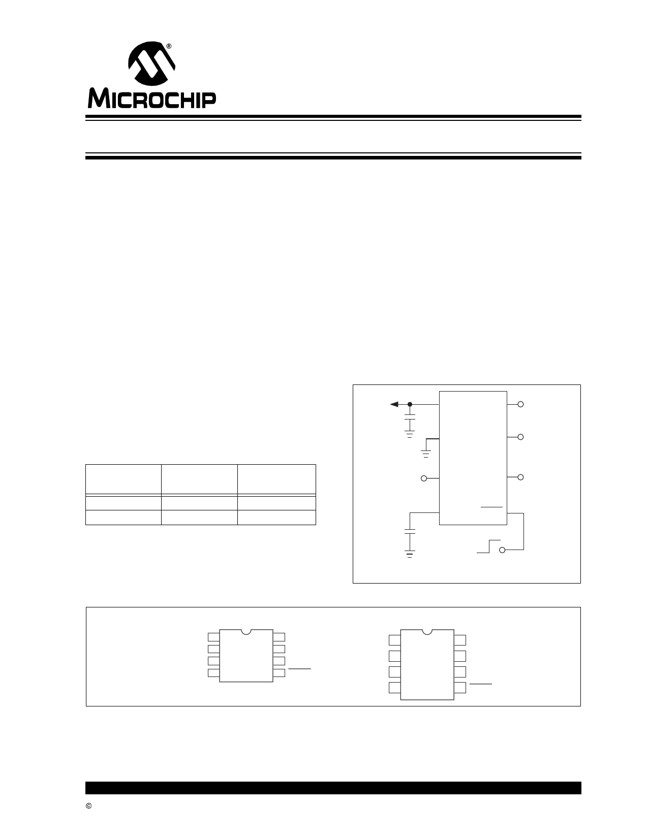
Typical Application
VOUT
1
+ C1 VOUT
1µF
2
GND
8
VIN
VIN
7
NC
TC1107
3 NC
6
NC
4
Bypass
SHDN 5
CBYPASS
470pF
(Optional)
Shutdown Control
(from Power Control Logic)
8-Pin SOIC
VOUT 1
8 VIN
GND 2
7 NC
TC1107VOA
NC 3
6 NC
Bypass 4
5 SHDN
© 2002 Microchip Technology Inc.
DS21356B-page 1
1 page 
4.0 THERMAL CONSIDERATIONS
4.1 Thermal Shutdown
Integrated thermal protection circuitry shuts the
regulator off when die temperature exceeds 150°C.
The regulator remains off until the die temperature
drops to approximately 140°C.
4.2 Power Dissipation
The amount of power the regulator dissipates is
primarily a function of input and output voltage, and
output current. The following equation is used to
calculate worst case actual power dissipation:
EQUATION 4-1:
PD ≈ (VINMAX – VOUTMIN)ILOADMAX
Where:
PD = Worst case actual power dissipation
VINMAX = Maximum voltage on VIN
VOUTMIN = Minimum regulator output voltage
ILOADMAX = Maximum output (load) current
The maximum allowable power dissipation (Equation
4-2) is a function of the maximum ambient temperature
(TAMAX), the maximum allowable die temperature
(TJMAX) and the thermal resistance from junction-to-air
(θJA). The 8-Pin SOIC package has a θJA of
approximately 160°C/Watt, while the 8-Pin MSOP
package has a θJA of approximately 200°C/Watt.
TC1107
EQUATION 4-2:
PDMAX = (TJMAX – TAMAX)
θJA
Where all terms are previously defined.
Equation 4-1 can be used in conjunction with Equation
4-2 to ensure regulator thermal operation is within
limits. For example:
Given:
VINMAX = 3.0V + 10%
VOUTMIN = 2.7V – 2.5%
ILOADMAX = 250mA
TJMAX = 125°C
TAMAX = 55°C
8-Pin MSOP Package
Find: 1. Actual power dissipation
2. Maximum allowable dissipation
Actual power dissipation:
PD ≈ (VINMAX – VOUTMIN)ILOADMAX
= [(3.0 x 1.1) – (2.7 x .975)]250 x 10–3
= 167mW
Maximum allowable power dissipation:
PDMAX = (TJMAX – TAMAX)
θJA
= (125 – 55)
220
= 318mW
In this example, the TC1107 dissipates a maximum of
167mW; below the allowable limit of 318mW. In a
similar manner, Equation 4-1 and Equation 4-2 can be
used to calculate maximum current and/or input
voltage limits.
4.3 Layout Considerations
The primary path of heat conduction out of the package
is via the package leads. Therefore, layouts having a
ground plane, wide traces at the pads, and wide power
supply bus lines combine to lower θJA and therefore
increase the maximum allowable power dissipation
limit.
© 2002 Microchip Technology Inc.
DS21356B-page 5
5 Page 
TC1107
Information contained in this publication regarding device
applications and the like is intended through suggestion only
and may be superseded by updates. It is your responsibility to
ensure that your application meets with your specifications.
No representation or warranty is given and no liability is
assumed by Microchip Technology Incorporated with respect
to the accuracy or use of such information, or infringement of
patents or other intellectual property rights arising from such
use or otherwise. Use of Microchip’s products as critical com-
ponents in life support systems is not authorized except with
express written approval by Microchip. No licenses are con-
veyed, implicitly or otherwise, under any intellectual property
rights.
Trademarks
The Microchip name and logo, the Microchip logo, FilterLab,
KEELOQ, microID, MPLAB, PIC, PICmicro, PICMASTER,
PICSTART, PRO MATE, SEEVAL and The Embedded Control
Solutions Company are registered trademarks of Microchip Tech-
nology Incorporated in the U.S.A. and other countries.
dsPIC, ECONOMONITOR, FanSense, FlexROM, fuzzyLAB,
In-Circuit Serial Programming, ICSP, ICEPIC, microPort,
Migratable Memory, MPASM, MPLIB, MPLINK, MPSIM,
MXDEV, MXLAB, PICC, PICDEM, PICDEM.net, rfPIC, Select
Mode and Total Endurance are trademarks of Microchip
Technology Incorporated in the U.S.A.
Serialized Quick Turn Programming (SQTP) is a service mark
of Microchip Technology Incorporated in the U.S.A.
All other trademarks mentioned herein are property of their
respective companies.
© 2002, Microchip Technology Incorporated, Printed in the
U.S.A., All Rights Reserved.
Printed on recycled paper.
© 2002 Microchip Technology Inc.
Microchip received QS-9000 quality system
certification for its worldwide headquarters,
design and wafer fabrication facilities in
Chandler and Tempe, Arizona in July 1999
and Mountain View, California in March 2002.
The Company’s quality system processes and
procedures are QS-9000 compliant for its
PICmicro® 8-bit MCUs, KEELOQ® code hopping
devices, Serial EEPROMs, microperipherals,
non-volatile memory and analog products. In
addition, Microchip’s quality system for the
design and manufacture of development
systems is ISO 9001 certified.
DS21356B-page 11
11 Page | ||
| Páginas | Total 12 Páginas | |
| PDF Descargar | [ Datasheet TC1107.PDF ] | |
Hoja de datos destacado
| Número de pieza | Descripción | Fabricantes |
| TC110 | PFM/PWM Step-Up DC/DC Controller | Microchip |
| TC110 | PFM/PWM Step-Up DC/DC Controller | Microchip Technology |
| TC1100H | (TC1xxxH) SURFACE MOUNT THYRISTOR SURGE PROTECTIVE DEVICE | Lite-On Technology |
| TC1100H | (TC1100H - TC1800H) SURFACE MOUNT THYRISTOR SURGE PROTECTIVE DEVICE | Lite-On |
| Número de pieza | Descripción | Fabricantes |
| SLA6805M | High Voltage 3 phase Motor Driver IC. |
Sanken |
| SDC1742 | 12- and 14-Bit Hybrid Synchro / Resolver-to-Digital Converters. |
Analog Devices |
|
DataSheet.es es una pagina web que funciona como un repositorio de manuales o hoja de datos de muchos de los productos más populares, |
| DataSheet.es | 2020 | Privacy Policy | Contacto | Buscar |