|
|
PDF 87974I Data sheet ( Hoja de datos )
| Número de pieza | 87974I | |
| Descripción | LVCMOS/LVTTL Clock Generator | |
| Fabricantes | IDT | |
| Logotipo |  |
|
Hay una vista previa y un enlace de descarga de 87974I (archivo pdf) en la parte inferior de esta página. Total 16 Páginas | ||
|
No Preview Available !
Low Skew, 1-to-15,
LVCMOS/LVTTL Clock Generator
87974I
Data Sheet
GENERAL DESCRIPTION
The 87974I is a low skew, low jitter 1-to-15 LVCMOS/
LVTTL Clock Generator/Zero Delay Buffer. The device
has a fully integrated PLL and three banks whose divider
ratios can be independently controlled, providing output
frequency relationships of 1:1, 2:1, 3:1, 3:2, 3:2:1. In
addition, the external feedback connection provides for a wide
selection of output-to-input frequency ratios. The CLK0 and
CLK1 pins allow for redundant clocking on the input and dynam-
ically switching the PLL between two clock sources.
Guaranteed low jitter and output skew characteristics make
the 87974I ideal for those applications demanding well defined
performance and repeatability.
FEATURES
• Fully integrated PLL
• Fifteen single ended 3.3V LVCMOS/LVTTL outputs
• Two LVCMOS/LVTTL clock inputs for redundant clock applica-
tions
• CLK0 and CLK1 accepts the following input levels:
LVCMOS/LVTTL
• Output frequency range: 8.33MHz to 125MHz
• VCO range: 200MHz to 500MHz
• External feedback for ”zero delay” clock regeneration
• Cycle-to-cycle jitter: ±100ps (typical)
• Output skew: 350ps (maximum)
• 3.3V operating supply
• -40°C to 85°C ambient operating temperature
• Available in lead-free RoHS-compliant package
PIN ASSIGNMENT
52-Lead LQFP
10mm x 10mm x 1.4mm package body
Y package
Top View
©2016 Integrated Device Technology, Inc
1
Revision E January 26, 2016
1 page 
87974I Data Sheet
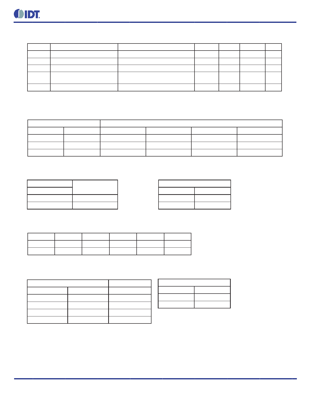
TABLE 2. PIN CHARACTERISTICS
Symbol Parameter
Test Conditions
CIN
RPULLUP
R
PULLDOWN
CPD
Input Capacitance
Input Pullup Resistor
Input Pulldown Resistor
Power Dissipation Capacitance
(per output); Note 1
VDD, VDDA, VDDOx = 3.465V
ROUT
Output Impedance
NOTE 1: VDDOx denotes VDDOA, VDDOB, VDDOC, VDDOFB.
Minimum
Typical
4
51
51
Maximum
Units
pF
KΩ
KΩ
15 pF
5 7 12 Ω
TABLE 3A. OUTPUT CONTROL PIN FUNCTION TABLE
Inputs
nMR/OE
CLK_EN
0X
10
11
QA0:QA4
HiZ
LOW
Enable
Outputs
QB0:QB4
QC0:QC3
HiZ HiZ
LOW
LOW
Enable
Enable
QFB
HiZ
Enable
Enable
TABLE 3B. OPERATING MODE FUNCTION TABLE
Inputs
PLL_SEL
0
1
Operating Mode
Bypass
PLL
TABLE 3C. PLL INPUT FUNCTION TABLE
Inputs
CLK_SEL
PLL Input
0 CLK0
1 CLK1
TABLE 3D. SELECT PIN FUNCTION TABLE
SEL_A
QAx
SEL_B
0 ÷2 0
1 ÷4 1
QBx
÷2
÷4
SEL_C
0
1
QCx
÷4
÷6
TABLE 3E. FB SELECT FUNCTION TABLE
Inputs
FB_SEL1
FB_SEL0
00
10
01
11
Outputs
QFB
÷4
÷6
÷8
÷ 12
TABLE 3F. VCO SELECT FUNCTION TABLE
Inputs
VCO_SEL
fVCO
0 VCO/2
1 VCO/4
©2016 Integrated Device Technology, Inc
5
Revision E January 26, 2016
5 Page 
87974I Data Sheet
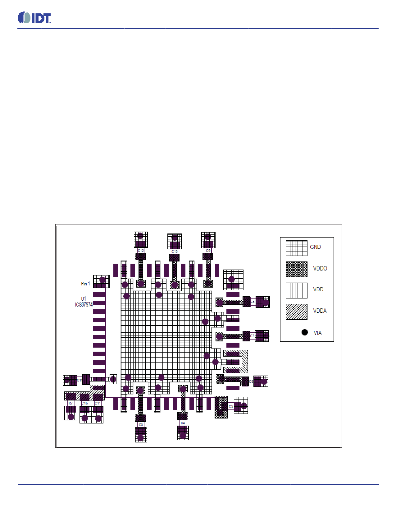
The following component footprints are used in this layout
example:
All the resistors and capacitors are size 0603.
POWER AND GROUNDING
Place the decoupling capacitors as close as possible to the pow-
er pins. If space allows, placement of the decoupling capacitor
on the component side is preferred. This can reduce unwanted
inductance between the decoupling capacitor and the power
pin caused by the via.
Maximize the power and ground pad sizes and number of vias
capacitors. This can reduce the inductance between the power
and ground planes and the component power and ground pins.
The RC filter consisting of R7, C11, and C16 should be placed
as close to the VDDA pin as possible.
CLOCK TRACES AND TERMINATION
Poor signal integrity can degrade the system performance or
cause system failure. In synchronous high-speed digital sys-
tems, the clock signal is less tolerant to poor signal integrity
than other signals. Any ringing on the rising or falling edge or
excessive ring back can cause system failure. The shape of the
trace and the trace delay might be restricted by the available
space on the board and the component location. While routing
the traces, the clock signal traces should be routed first and
should be locked prior to routing other signal traces.
• The differential 50Ω output traces should have same
length.
• Avoid sharp angles on the clock trace. Sharp angle turns
cause the characteristic impedance to change on the
transmission lines.
• Keep the clock traces on the same layer. Whenever pos-
sible, avoid placing vias on the clock traces. Placement
of vias on the traces can affect the trace characteristic
impedance and hence degrade signal integrity.
• To prevent cross talk, avoid routing other signal traces
in parallel with the clock traces. If running parallel traces
is unavoidable, allow a separation of at least three trace
widths between the differential clock trace and the other
signal trace.
• Make sure no other signal traces are routed between
the clock trace pair.
• The series termination resistors should be located as
close to the driver pins as possible.
FIGURE 2B. PCB BOARD LAYOUT FOR 87974I
©2016 Integrated Device Technology, Inc
11
Revision E January 26, 2016
11 Page | ||
| Páginas | Total 16 Páginas | |
| PDF Descargar | [ Datasheet 87974I.PDF ] | |
Hoja de datos destacado
| Número de pieza | Descripción | Fabricantes |
| 87974I | LVCMOS/LVTTL Clock Generator | IDT |
| Número de pieza | Descripción | Fabricantes |
| SLA6805M | High Voltage 3 phase Motor Driver IC. |
Sanken |
| SDC1742 | 12- and 14-Bit Hybrid Synchro / Resolver-to-Digital Converters. |
Analog Devices |
|
DataSheet.es es una pagina web que funciona como un repositorio de manuales o hoja de datos de muchos de los productos más populares, |
| DataSheet.es | 2020 | Privacy Policy | Contacto | Buscar |
