|
|
PDF NB3W800L Data sheet ( Hoja de datos )
| Número de pieza | NB3W800L | |
| Descripción | 3.3V 100/133MHz Differential 1:8 HCSLCompatible Push-Pull Clock ZDB/Fanout Buffer | |
| Fabricantes | ON Semiconductor | |
| Logotipo | ||
Hay una vista previa y un enlace de descarga de NB3W800L (archivo pdf) en la parte inferior de esta página. Total 17 Páginas | ||
|
No Preview Available !
NB3W800L
3.3 V 100/133 MHz
Differential 1:8 HCSL-
Compatible Push-Pull Clock
ZDB/Fanout Buffer for PCIe)
Description
The NB3W800L is a low−power 8−output differential buffer that
meets all the performance requirements of the DB800ZL
specification. The NB3W800L is capable of distributing the reference
clocks for Intel® QuickPath Interconnect (Intel QPI), PCIe
Gen1/Gen2/Gen3, SAS, SATA, and Intel Scalable Memory Interconnect
(Intel SMI) applications. A fixed, internal feedback path maintains low
drift for critical QPI applications.
Features
• 8 Differential Clock Output Pairs @ 0.7 V
• Low−power NMOS Push−pull HCSL Compatible Outputs
• Cycle−to−cycle Jitter <50 ps
• Output−to−output Skew <50 ps
• Input−to−output Delay Variation <100 ps
• PCIe Gen3 Phase Jitter <1.0 ps RMS
• QPI 9.6GT/s 12UI Phase Jitter <0.2 ps RMS
• Pseudo−External Fixed Feedback for Lowest Input−to−output Delay
• Individual OE Control; Hardware Control of Each Output
• PLL Configurable for PLL Mode or Bypass Mode (Fanout
Operation)
• 100 MHz or 133 MHz PLL Mode Operation; Supports PCIe and QPI
Applications
• Selectable PLL Bandwidth; Minimizes Jitter Peaking in Downstream
PLL’s
• SMBus Programmable Configurations
• Spread Spectrum Compatible; Tracks Input Clock Spreading for Low
EMI
• These are Pb−Free Devices
www.onsemi.com
1 48
CASE 485DP
MARKING
DIAGRAM
1
NB3W800L
AWLYYWWG
NB3W800L = Specific Device Code
A = Assembly Location
WL = Wafer Lot
YY = Year
WW = Work Week
G = Pb−Free Package
ORDERING INFORMATION
Device
Package
Shipping†
NB3W800LMNG
QFN48
(Pb−Free)
490 / Tray
NB3W800LMNTXG QFN48 2500 / Tape &
(Pb−Free)
Reel
NB3W800LMNTWG QFN48 2500 / Tape &
(Pb−Free)
Reel
†For information on tape and reel specifications,
including part orientation and tape sizes, please
refer to our Tape and Reel Packaging Specification
Brochure, BRD8011/D.
© Semiconductor Components Industries, LLC, 2016
July, 2016 − Rev. 2
1
Publication Order Number:
NB3W800L/D
1 page 
NB3W800L
Table 9. ABSOLUTE MAXIMUM RATINGS
Symbol
Parameter
Conditions
Min Typ Max Units
VDD, VDDA
3.3 V Supply Voltage (Notes 1, 2)
VDD for core logic and PLL
4.6 V
VIL
VIH
VIHSMB
Ts
Input Low Voltage (Note 1)
Input High Voltage (Note 1)
Input High Voltage (Note 1)
Storage Temperature (Note 1)
Except for SMBus interface
SMBus clock and data pins
GND−0.5
−65
VDD + 0.5
5.5
150
V
V
V
°C
Tj Junction Temperature (Note 1)
125 °C
ESD prot
Input ESD protection (Note 1)
Human Body Model
2000
V
qJA Thermal Resistance, Junction−to−Ambient
Still air
17 °C/W
qJC Thermal Resistance, Junction−to−Case
7 °C/W
Stresses exceeding those listed in the Maximum Ratings table may damage the device. If any of these limits are exceeded, device functionality
should not be assumed, damage may occur and reliability may be affected.
1. Guaranteed by design and characterization, not tested in production.
2. Operation under these conditions is neither implied nor guaranteed.
Table 10. ELECTRICAL CHARACTERISTICS–CLOCK INPUT PARAMETERS (HCSL−COMPATIBLE)
(VDD = VDDA = 3.3 V ±5%, TA = 0°C * 70°C), See Test Loads for Loading Conditions. (Note 5)
Symbol
Parameter
Conditions
Min Typ
Max
Units
VIHCLK_IN
Input High Voltage - CLK_IN (Note 3)
Differential inputs
(single−ended measurement)
600
800
1150
mV
VILCLK_IN
Input Low Voltage - CLK_IN (Note 3)
Differential inputs
(single−ended measurement)
VSS - 300
0
300 mV
VCOM
Input Common Mode
Voltage - CLK_IN (Note 3)
Common Mode Input Voltage
(Single−ended measurement)
300
1000
mV
VSWING
dv/dt
Input Amplitude - CLK_IN (Note 3)
Input Slew Rate - CLK_IN (Notes 3, 4)
Peak to Peak (differential)
Measured differentially
300
0.35
1450
8
mV
V/ns
IIN Input Leakage Current (Note 3)
VIN = VDD , VIN = GND
−5
dtin
Input Duty Cycle (Note 3)
Measurement from differential
45
waveform
5 mA
55 %
JDIFIn
Input Jitter - Cycle to Cycle (Note 3)
Differential Measurement
125 ps
Product parametric performance is indicated in the Electrical Characteristics for the listed test conditions, unless otherwise noted. Product
performance may not be indicated by the Electrical Characteristics if operated under different conditions.
3. Guaranteed by design and characterization, not tested in production.
4. Slew rate measured through ±75 mV window centered around differential zero.
5. Test configuration is; Rs = 27 W, 2 pF for 85 W transmission line.
www.onsemi.com
5
5 Page 
Vovs
VHigh
Vrb
NB3W800L
Measurement Points for Differential
Vrb
VLow
Vuds
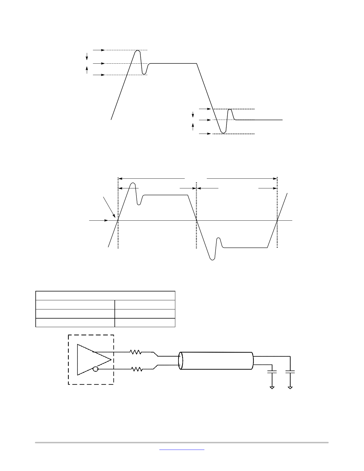
Figure 4. Single−Ended Measurement Points for Vovs, Vuds, Vrb
Skew measurement point
High Duty Cycle%
TPeriod
Low Duty Cycle%
0.0 V
Figure 5. Differential (DIFFX – DIFFX#) Measurement Points (Tperiod, Duty Cycle, Jitter)
Test Loads
Differential Output Terminations
DIF Zo (W)
Rs (W)
100 33
85 27
Low−Power
HCSL−
Compatible
Output Buffer
Rs 10 inches
85 W Differential Zo
Rs
Figure 6. Differential Test Loads
2 pF 2 pF
www.onsemi.com
11
11 Page | ||
| Páginas | Total 17 Páginas | |
| PDF Descargar | [ Datasheet NB3W800L.PDF ] | |
Hoja de datos destacado
| Número de pieza | Descripción | Fabricantes |
| NB3W800L | 3.3V 100/133MHz Differential 1:8 HCSLCompatible Push-Pull Clock ZDB/Fanout Buffer | ON Semiconductor |
| Número de pieza | Descripción | Fabricantes |
| SLA6805M | High Voltage 3 phase Motor Driver IC. |
Sanken |
| SDC1742 | 12- and 14-Bit Hybrid Synchro / Resolver-to-Digital Converters. |
Analog Devices |
|
DataSheet.es es una pagina web que funciona como un repositorio de manuales o hoja de datos de muchos de los productos más populares, |
| DataSheet.es | 2020 | Privacy Policy | Contacto | Buscar |
