|
|
|
PDF 74AUP1G17 Data sheet ( Hoja de datos )
| Número de pieza | 74AUP1G17 | |
| Descripción | SINGLE SCHMITT-TRIGGER BUFFER | |
| Fabricantes | Diodes | |
| Logotipo | ||
Hay una vista previa y un enlace de descarga de 74AUP1G17 (archivo pdf) en la parte inferior de esta página. Total 14 Páginas | ||
|
No Preview Available !
74AUP1G17
SINGLE SCHMITT-TRIGGER BUFFER
Description
The Advanced Ultra Low Power (AUP) CMOS logic family is designed
for low power and extended battery life in portable applications.
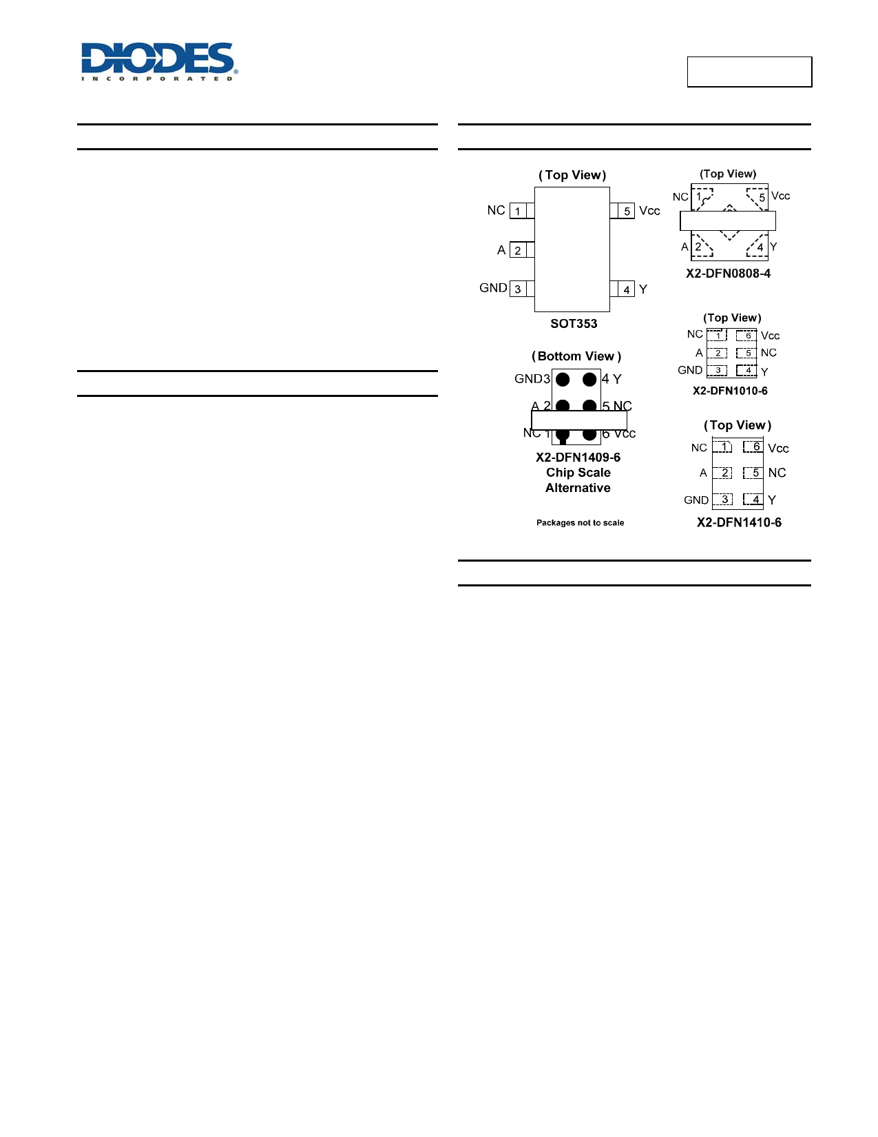
Pin Assignments
The AUP1G17 is a single 1-input Schmitt-trigger buffer gate with a
push-pull output designed for operation over a power supply range of
0.8V to 3.6V. The device is fully specified for partial power down
applications using IOFF. The IOFF circuitry disables the output
preventing damaging current backflow when the device is powered
down.
The gate performs the positive Boolean function:
YA
Future Product
Features
Advanced Ultra Low Power (AUP) CMOS
Supply Voltage Range from 0.8V to 3.6V
±4mA Output Drive at 3.0V
Low Static power consumption
Icc < 0.9µA
Low Dynamic Power Consumption
CPD = 6pF (Typical at 3.6)
Schmitt Trigger Action at All Inputs Make the Circuit Tolerant for
Slower Input Rise and Fall Time. The hysteresis is typically
250mV at Vcc = 3.0V
IOFF Supports Partial-Power-Down Mode Operation
ESD Protection Exceeds JESD 22
2000-V Human Body Model (A114-A)
Exceeds 1000-V Charged Device Model (C101C)
Latch-Up Exceeds 100mA per JESD 78, Class II
Leadless packages named per JESD30E
Totally Lead-Free & Fully RoHS Compliant (Notes 1 & 2)
Halogen and Antimony Free. “Green” Device (Note 3)
Future Product
Applications
Suited for battery and low power needs
Wide array of products such as:
Tablets, E-readers
Cell Phones, Personal Navigation / GPS
MP3 players ,Cameras, Video Recorders
PCs ultrabooks, notebooks, netbooks,
Computer peripherals, hard drives, CD/DVD ROM
TV, DVD, DVR, set top box
Notes:
1. No purposely added lead. Fully EU Directive 2002/95/EC (RoHS) & 2011/65/EU (RoHS 2) compliant.
2. See http://www.diodes.com for more information about Diodes Incorporated’s definitions of Halogen- and Antimony-free, "Green" and Lead-free.
3. Halogen- and Antimony-free "Green” products are defined as those which contain <900ppm bromine, <900ppm chlorine (<1500ppm total Br + Cl) and
<1000ppm antimony compounds.
Click here for ordering information, located at the end of datasheet
74AUP1G17
Document number: DS35153 Rev. 2 - 2
1 of 14
www.diodes.com
July 2013
© Diodes Incorporated
1 page 
74AUP1G17
Electrical Characteristics (cont.) (@TA = +25°C, unless otherwise specified.)
Symbol Parameter
Test Conditions
Positive-going
VT+ input threshold
voltage
Negative-going
VT- input threshold
voltage
ΔVT
Hysteresis
(VT+ - VT-)
VOH
VOL
II
IOFF
ΔIOFF
ICC
ΔICC
IOH = -20μA
IOH = -1.1mA
IOH = -1.7mA
High_Level
Output Voltage
IOH = -1.9mA
IOH = -2.3mA
IOH = -3.1mA
IOH = -2.7mA
IOH = -4mA
IOL = 20μA
IOL = 1.1mA
IOL = 1.7mA
Low-Level Output IOL = 1.9mA
Voltage
IOL = 2.3mA
IOL = 3.1mA
IOL = 2.7mA
IOL = 4mA
Input Current
VI = GND to 3.6V
Power Down
Leakage Current
VI or VO = 0V to 3.6V
Delta Power
Down Leakage
Current
VI or VO = 0V to 3.6V
Supply Current VI = GND or VCC, IO =
0
Additional Supply
Current
Input at VCC -0.6V
VCC
0.8V
1.1V
1.4V
1.65V
2.3V
3.0V
0.8V
1.1V
1.4V
1.65V
2.3V
3.0V
0.8V
1.1V
1.4V
1.65V
2.3V
3.0V
0.8V to 3.6V
1.1V
1.4V
1.65V
2.3V
3V
0.8V to 3.6V
1.1V
1.4V
1.65V
2.3V
3V
0V to 3.6V
0
0V to 0.2V
0.8V to 3.6V
3.3V
TA = -40°C to +125°C
Min Max
0.4 0.65
0.53 0.9
0.74 1.11
0.91 1.29
1.37 1.77
1.61 2.32
0.15 0.4
0.26 0.65
0.39 0.75
0.47 0.84
0.69 1.04
0.88 1.24
0.07 0.5
0.08 0.46
0.18 0.56
0.27 0.66
0.53 0.92
0.79 1.31
VCC – 0.11
0.6 X VCC
0.93
1.17
1.77
1.67
2.40
2.30
0.11
0.33 X VCC
0.41
0.39
0.36
0.50
0.36
0.50
± 0.75
± 3.5
± 2.5
3.0
75
Unit
V
V
V
V
V
μA
μA
μA
μA
μA
74AUP1G17
Document number: DS35153 Rev. 2 - 2
5 of 14
www.diodes.com
July 2013
© Diodes Incorporated
5 Page 
74AUP1G17
Package Outline Dimensions (cont.) (All dimensions in mm.)
Please see AP02002 at http://www.diodes.com/datasheets/ap02002.pdf for latest version.
(3) X2-DFN1010-6
A A1
A3
(Pin #1 ID)
b1
E
L(6x)
Z(4x)
D
e
K
b(6x)
X2-DFN1010-6
Dim Min Max
Typ
A –– 0.40 0.39
A1 0.00 0.05 0.02
A3 –– –– 0.13
b 0.14 0.20 0.17
b1 0.05 0.15 0.10
D 0.95 1.05 1.00
E 0.95 1.05 1.00
e –– –– 0.35
L 0.35 0.45 0.40
K 0.15 ––
––
Z –– –– 0.065
All Dimensions in mm
(4) X2-DFN1409-6
A
Pin # 1 I D
E
D
e1
A3
A1
S e a ti n g P l a n e
Ø 6x
e2
Z1 4x
Z2 4x
X2-DFN1409-6
Dim Min Max
Typ
A - 0.40 0.39
A1 0 0.05 0.02
A3 -
- 0.13
Ø 0.20 0.30 0.25
D 1.35 1.45 1.40
E 0.85 0.95 0.90
e1 -
- 0.50
e2 -
- 0.50
Z1 -
- 0.075
Z2 -
- 0.075
All Dimensions in mm
74AUP1G17
Document number: DS35153 Rev. 2 - 2
11 of 14
www.diodes.com
July 2013
© Diodes Incorporated
11 Page | ||
| Páginas | Total 14 Páginas | |
| PDF Descargar | [ Datasheet 74AUP1G17.PDF ] | |
Hoja de datos destacado
| Número de pieza | Descripción | Fabricantes |
| 74AUP1G11 | Low-power 3-input AND gate | NXP Semiconductors |
| 74AUP1G125 | Low-power buffer/line driver 3-state | NXP Semiconductors |
| 74AUP1G125 | SINGLE BUFFER GATE | Diodes |
| 74AUP1G126 | Low-Power buffer/line driver 3-state | NXP Semiconductors |
| Número de pieza | Descripción | Fabricantes |
| SLA6805M | High Voltage 3 phase Motor Driver IC. |
Sanken |
| SDC1742 | 12- and 14-Bit Hybrid Synchro / Resolver-to-Digital Converters. |
Analog Devices |
|
DataSheet.es es una pagina web que funciona como un repositorio de manuales o hoja de datos de muchos de los productos más populares, |
| DataSheet.es | 2020 | Privacy Policy | Contacto | Buscar |