|
|
|
PDF NB3L853141 Data sheet ( Hoja de datos )
| Número de pieza | NB3L853141 | |
| Descripción | 2.5V/3.3V 1:5 LVPECL Fanout Buffer | |
| Fabricantes | ON Semiconductor | |
| Logotipo | ||
Hay una vista previa y un enlace de descarga de NB3L853141 (archivo pdf) en la parte inferior de esta página. Total 10 Páginas | ||
|
No Preview Available !
NB3L853141
2.5V/3.3V 1:5 LVPECL
Fanout Buffer
Description
The NB3L853141 is a low skew 1:5 LVPECL Clock fanout buffer
designed explicitly for low output skew applications.
The NB3L853141 features a multiplexed input which can be driven
by either a differential or single−ended input to allow for the
distribution of a lower speed clock along with the high speed system
clock.
The SEL pin will select the differential clock inputs, CLK0 &
CLK0, when LOW (or left open and pulled LOW by the internal
pull−down resistor). When SEL is HIGH, the single−ended CLK1
input is selected.
The common enable (EN) is synchronous so that the outputs will
only be enabled/disabled when they are already in the LOW state. This
avoids any chance of generating a runt clock pulse when the device is
enabled/disabled as can happen with an asynchronous control. The
internal flip flop is clocked on the falling edge of the input clock,
therefore, all associated specification limits are referenced to the
negative edge of the clock input.
Features
• 700 MHz Maximum Clock Output Frequency
• CLK0 and CLK0 can Accept Differential LVPECL, LVDS, HCSL,
LVHSTL, SSTL, LVCMOS
• CLK1 can Accept LVCMOS and LVTTL
• Five Differential LVPECL Clock Outputs
• 1.5 ns Maximum Propagation Delay
• Operating Range: VCC = 2.375 V to 3.8 V
• LVCMOS Compatible Control Inputs
• Selectable Differential or LVCMOS Clock Inputs
• Synchronous Clock Enable
• 30 ps Max. Skew Between Outputs
• −40°C to +85°C Ambient Operating Temperature Range
• TSSOP−20 Package
• These are Pb−Free Devices
Applications
• Computing and Telecom
• Routers, Servers and Switches
• Backplanes
www.onsemi.com
MARKING
DIAGRAM
TSSOP−20
DT SUFFIX
CASE 948E
NB3L
3141
ALYW
A = Assembly Location
WL = Wafer Lot
YY = Year
WW = Work Week
G = Pb−Free Package
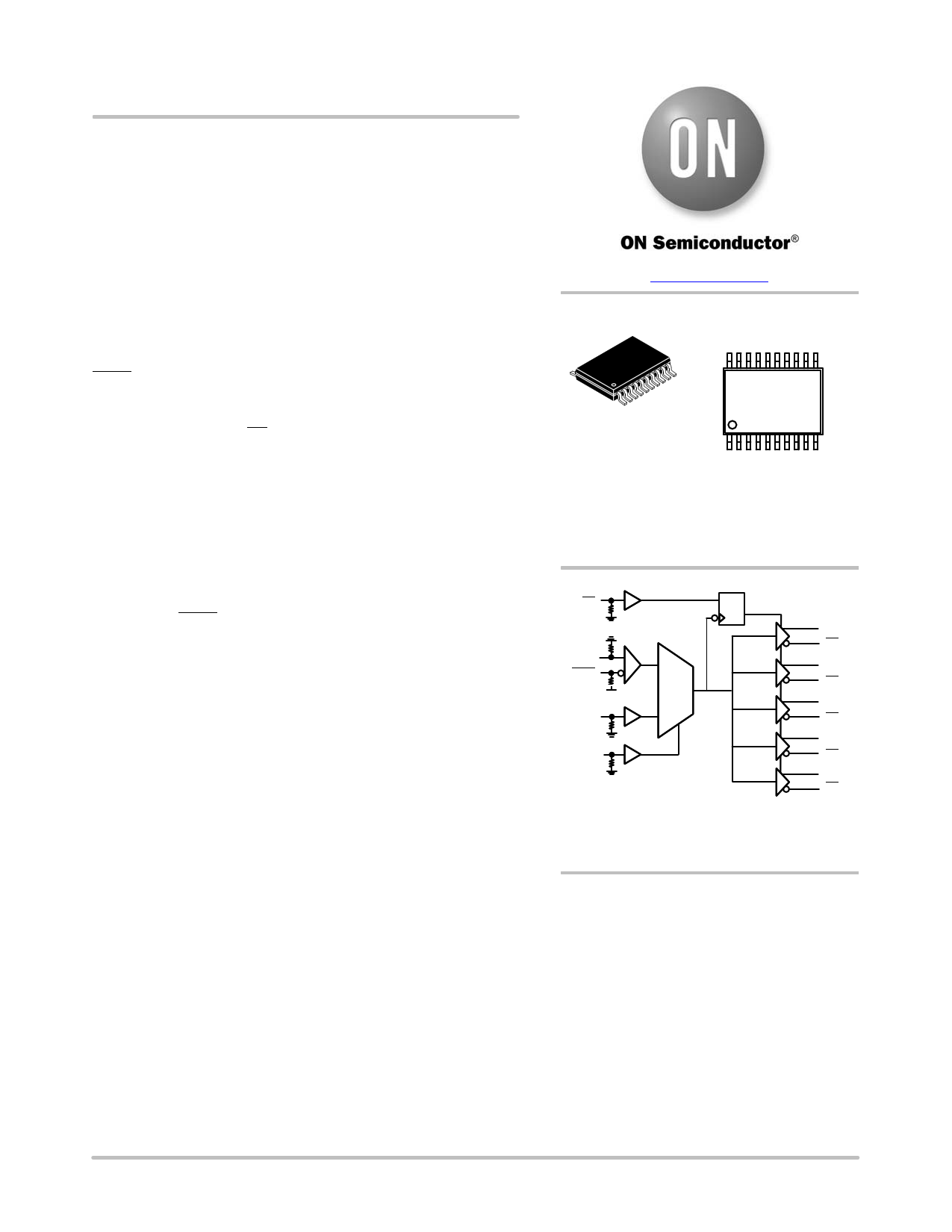
EN
CLK0
CLK0
+
CLK1
SEL
0
1
D
Q
Q0
Q0
Q1
Q1
Q2
Q2
Q3
Q3
Q4
Q4
Figure 1. Simplified Logic Diagram of
NB3L853141
ORDERING INFORMATION
See detailed ordering and shipping information on page 8 of
this data sheet.
© Semiconductor Components Industries, LLC, 2015
December, 2015 − Rev. 2
1
Publication Order Number:
NB3L853141/D
1 page 
NB3L853141
Table 6. AC CHARACTERISTICS, VCC = 2.375 V to 3.8 V, TA = −40°C to +85°C (Note 8)
Symbol
Characteristic
fMAX
Maximum Input Clock Frequency: VOUTpp ≥ 400 mV CLK0/CLK0, VINPPmin ≥ 250 mV
CLK1
Min
700
300
Typ Max Unit
MHz
FN Phase Noise, fC = 155.52 MHz
10 Hz
100 Hz
1 kHz
10 kHz
100 kHz
1 MHz
10 MHz
20 MHz
Offset from Carrier
−100.5
−128.2
−138.6
−147.1
−149.7
−154.2
−154.2
−154.2
dBc/
Hz
tPLH,
tPHL
Propagation Delay to Differential Outputs, @ 50 MHz Note 9
Note 10
CLK0/CLK0 to Q/Q
CLK1 to Q
0.8
0.8
1.0 1.5 ns
1.0 1.5
t∫FN Additive Phase Jitter, RMS; fC = 155.52 MHz,
Integration Range: 12 kHz − 20 MHz
0.05 ps
tsk(o) Output−to−output skew; (Note 11)
30 ps
tsk (pp) Part−to−Part Skew; (Note 12)
150 ps
VINpp
tr/tf
ODC
Input Voltage Swing/Sensitivity (Differential Configuration) (Note 14)
Output rise and fall times, 20% to 80%,
Q, Q
Output Clock Duty Cycle
Input Duty Cycle = 50%
CLK0/CLK0, f ≤ 700 MHz, VINPPmin ≥ 250 mV
CLK1, f ≤ 250MHz
150
200
45
45
1300
700
55
55
mV
ps
%
All parameters measured at fMAX unless noted otherwise.
The cycle−to−cycle jitter on the input will equal the jitter on the
output. The part does not add jitter
8. Measured using a VINPPmin source, Reference Duty Cycle = 50% duty cycle clock source. All output loading with external 50 W to VCC * 2 V.
9. Measured from the differential input crossing point to the differential output crossing point.
10. Measured from VCC /2 input crossing point to the differential output crossing point.
11. Defined as skew between outputs at the same supply voltage and with equal load conditions. Measured at the output differential cross points.
12. Defined as skew between outputs on different devices operating at the same supply voltages and with equal load conditions. Using the same
type of inputs on each device, the outputs are measured at the differential cross points.
13. Output voltage swing is a single−ended measurement operating in differential mode.
14. Input voltage swing is a single−ended measurement operating in differential mode.
www.onsemi.com
5
5 Page | ||
| Páginas | Total 10 Páginas | |
| PDF Descargar | [ Datasheet NB3L853141.PDF ] | |
Hoja de datos destacado
| Número de pieza | Descripción | Fabricantes |
| NB3L853141 | 2.5V/3.3V 1:5 LVPECL Fanout Buffer | ON Semiconductor |
| Número de pieza | Descripción | Fabricantes |
| SLA6805M | High Voltage 3 phase Motor Driver IC. |
Sanken |
| SDC1742 | 12- and 14-Bit Hybrid Synchro / Resolver-to-Digital Converters. |
Analog Devices |
|
DataSheet.es es una pagina web que funciona como un repositorio de manuales o hoja de datos de muchos de los productos más populares, |
| DataSheet.es | 2020 | Privacy Policy | Contacto | Buscar |