|
|
|
PDF B9948L Data sheet ( Hoja de datos )
| Número de pieza | B9948L | |
| Descripción | 1:12 Clock Distribution Buffer | |
| Fabricantes | Cypress Semiconductor | |
| Logotipo | ||
Hay una vista previa y un enlace de descarga de B9948L (archivo pdf) en la parte inferior de esta página. Total 6 Páginas | ||
|
No Preview Available !
B9948L
2.5V/3.3V, 160-MHz, 1:12 Clock Distribution Buffer
Product Features
• 160-MHz clock support
• 2.5V or 3.3V output capability
• 200-ps maximum output-to-output skew
• LVPECL or LVCMOS/LVTTL clock input
• LVCMOS/LVTTL compatible inputs
• 12 clock outputs: drive up to 24 clock lines
• Synchronous Output Enable
• Output Three-state control
• Pin compatible with MPC948L
• Industrial temp. range: –40°C to +85°C
• 32-pin TQFP package
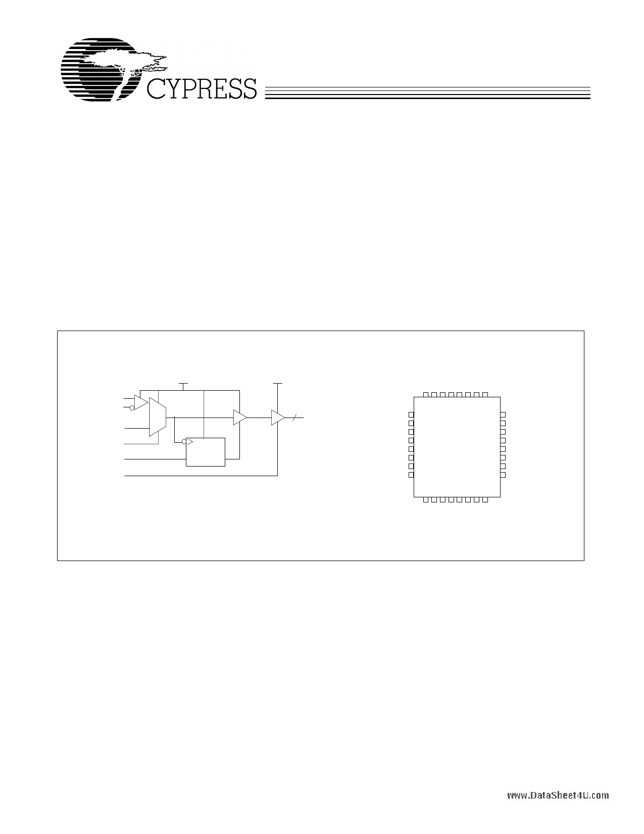
Block Diagram
Description
The B9948L is a low-voltage clock distribution buffer with the
capability to select either a differential LVPECL or a LVCMOS/
LVTTL compatible input clock. The two clock sources can be
used to provide for a test clock as well as the primary system
clock. All other control inputs are LVCMOS/LVTTL compatible.
The twelve outputs are 2.5V or 3.3V LVCMOS or LVTTL com-
patible and can drive two series-terminated 50Ω transmission
lines. With this capability the B9948L has an effective fanout
of 1:24. The outputs can also be three-stated via the three-
state input TS#. Low output-to-output skews make the B9948L
an ideal clock distribution buffer for nested clock trees in the
most demanding of synchronous systems.
The B9948L also provides a synchronous output enable input
for enabling or disabling the output clocks. Since this input is
internally synchronized to the input clock, potential output
glitching or runt pulse generation is eliminated.
Pin Configuration
PECL_CLK
PECL_CLK#
TCLK
TCLK_SEL
SYNC_OE
TS#
VDD
0
1
VDDC
12 Q0-Q11
TCLK_SEL
TCLK
PECL_CLK
PECL_CLK#
SYNC_OE
TS#
VDD
VSS
1 24 VSS
2 23 Q4
3 22 VDDC
B9948L4 21 Q5
5 20 VSS
6 19 Q6
7 18 VDDC
8 17 Q7
www.DataSheet4U.com
Cypress Semiconductor Corporation • 3901 North First Street • San Jose • CA 95134 • 408-943-2600
Document #: 38-07080 Rev. *C
Revised December 21, 2002
1 page 
Package Drawing and Dimensions
D
D1
L
12°
e
A1
b
B9948L
32-Pin TQFP Outline Dimensions
Symbol
A
A1
A2
D
D1
b
e
L
Inches
Min. Nom. Max.
- - 0.047
0.002 - 0.006
0.037 - 0.041
- 0.354 -
- 0.276 -
0.012 - 0.018
0.031 BSC
0.018 - 0.030
Ml
Min. Nom. Max.
- - 1.20
0.05 - 0.15
0.95 - 1.05
- 9.00 -
- 7.00 -
0.30 - 0.45
0.80 BSC
0.45 - 0.75
www.DataSheet4U.com
Document #: 38-07080 Rev. *C
Page 5 of 6
© Cypress Semiconductor Corporation, 2002. The information contained herein is subject to change without notice. Cypress Semiconductor Corporation assumes no responsibility for the use
of any circuitry other than circuitry embodied in a Cypress Semiconductor product. Nor does it convey or imply any license under patent or other rights. Cypress Semiconductor does not authorize
its products for use as critical components in life-support systems where a malfunction or failure may reasonably be expected to result in significant injury to the user. The inclusion of Cypress
Semiconductor products in life-support systems application implies that the manufacturer assumes all risk of such use and in doing so indemnifies Cypress Semiconductor against all charges.
5 Page | ||
| Páginas | Total 6 Páginas | |
| PDF Descargar | [ Datasheet B9948L.PDF ] | |
Hoja de datos destacado
| Número de pieza | Descripción | Fabricantes |
| B9948 | 1:12 Clock Distribution Buffer | Cypress Semiconductor |
| B9948L | 1:12 Clock Distribution Buffer | Cypress Semiconductor |
| Número de pieza | Descripción | Fabricantes |
| SLA6805M | High Voltage 3 phase Motor Driver IC. |
Sanken |
| SDC1742 | 12- and 14-Bit Hybrid Synchro / Resolver-to-Digital Converters. |
Analog Devices |
|
DataSheet.es es una pagina web que funciona como un repositorio de manuales o hoja de datos de muchos de los productos más populares, |
| DataSheet.es | 2020 | Privacy Policy | Contacto | Buscar |