|
|
|
PDF ICS8305I Data sheet ( Hoja de datos )
| Número de pieza | ICS8305I | |
| Descripción | MULTIPLEXED DIFFERENTIAL/LVCMOS-TO-LVCMOS/LVTTL FANOUT BUFFER | |
| Fabricantes | Integrated Circuit Systems | |
| Logotipo | ||
Hay una vista previa y un enlace de descarga de ICS8305I (archivo pdf) en la parte inferior de esta página. Total 15 Páginas | ||
|
No Preview Available !
Integrated
Circuit
Systems, Inc.
ICS8305I
LOW SKEW, 1-TO-4, MULTIPLEXED DIFFERENTIAL/
LVCMOS-TO-LVCMOS/LVTTL FANOUT BUFFER
GENERAL DESCRIPTION
The ICS8305I is a low skew, 1-to-4, Differential/
ICS LVCMOS-to-LVCMOS/LVTTL Fanout Buffer and a
HiPerClockS™ member of the HiPerClockS™ family of High
Performance Clock Solutions from ICS. The
ICS8305I has selectable clock inputs that accept
either differential or single ended input levels.The clock enable is
internally synchronized to eliminate runt pulses on the outputs
during asynchronous assertion/deassertion of the clock enable
www.DataSheept4inU..Ocoumtputs are forced LOW when the clock is disabled. A sepa-
rate output enable pin controls whether the outputs are in the
active or high impedance state.
Guaranteed output and part-to-part skew characteristics make
the ICS8305I ideal for those applications demanding well de-
fined performance and repeatability.
FEATURES
• 4 LVCMOS/LVTTL outputs
• Selectable differential or LVCMOS/LVTTL clock inputs
• CLK, nCLK pair can accept the following differential
input levels: LVPECL, LVDS, LVHSTL, HCSL, SSTL
• LVCMOS_CLK supports the following input types:
LVCMOS, LVTTL
• Maximum output frequency: 350MHz
• Output skew: 40ps (maximum)
• Part-to-part skew: 700ps (maximum)
• Additive phase jitter, RMS: 0.04ps (typical)
• 3.3V core, 3.3V, 2.5V or 1.8V output operating supply
• -40°C to 85°C ambient operating temperature
• Lead-Free package fully RoHS compliant
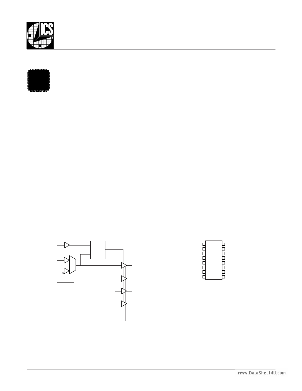
BLOCK DIAGRAM
CLK_EN
LVCMOS_CLK
CLK
nCLK
CLK_SEL
00
11
D
Q
LE
OE
PIN ASSIGNMENT
GND 1 16 Q0
OE 2
15 VDDO
VDD 3
14 Q1
CLK_EN 4 13 GND
CLK 5 12 Q2
Q0
nCLK 6
11 VDDO
CLK_SEL 7 10 Q3
Q1
LVCMOS_CLK 8
9 GND
Q2 ICS8305I
16-Lead TSSOP
4.4mm x 3.0mm x 0.92mm package body
Q3 G Package
Top View
8305AGI
www.icst.com/products/hiperclocks.html
1
REV. B MAY 19, 2005
1 page 
Integrated
Circuit
Systems, Inc.
ICS8305I
LOW SKEW, 1-TO-4, MULTIPLEXED DIFFERENTIAL/
LVCMOS-TO-LVCMOS/LVTTL FANOUT BUFFER
TABLE 4C. DIFFERENTIAL DC CHARACTERISTICS, VDD = 3.3V±5%, TA = -40°C TO 85°C
Symbol Parameter
Test Conditions
Minimum Typical
nCLK
IIH
Input High Current
CLK
VIN = VDD = 3.465V
VIN = VDD = 3.465V
nCLK
IIL
Input Low Current
CLK
VIN = 0V, VDD = 3.465V
VIN = 0V, VDD = 3.465V
-150
-5
VPP
www.DataSheet4U.com
VCMR
Peak-to-Peak Input Voltage
Common Mode Input Voltage;
NOTE 1, 2
0.15
GND + 0.5
NOTE 1: For single ended applications, the maximum input voltage for CLK, nCLK is VDD + 0.3V.
NOTE 2: Common mode voltage is defined as VIH.
Maximum
150
150
1.3
VDD - 0.85
Units
µA
µA
µA
µA
V
V
TABLE 5A. AC CHARACTERISTICS, VDD = VDDO = 3.3V ± 5%, TA = -40°C TO 85°C
Symbol Parameter
Test Conditions
Minimum Typical Maximum Units
fMAX
tpLH
tsk(o)
Output Frequency
Propagation Delay,
Low to High
LVCMOS_CLK;
NOTE 1A
CLK, nCLK;
NOTE 1B
Output Skew; NOTE 2, 6
Ref = CLK/nCLK
Ref = LVCMOS_CLK
Measured on the Rising Edge
1.75
350 MHz
300 MHz
2.8 ns
40 ps
tsk(pp)
tjit
tR / tF
odc
Part-to-Part Skew; NOTE 3, 6
Buffer Additive Phase Jitter, RMS;
refer to Additive Phase Jitter section,
NOTE 5
Output Rise/Fall Time
Output Duty Cycle
20% to 80%
IJ 200MHz
ƒ> 200MHz
700 ps
0.04 ps
100 700 ps
45 55 %
42 58 %
tEN Output Enable Time; NOTE 4
tDIS Output Disable Time; NOTE 4
NOTE 1A: Measured from the VDD/2 of the input to VDDO/2 of the output.
NOTE 1B: Measured from the differential input crossing point to VDDO/2 of the output.
NOTE 2: Defined as skew between outputs at the same supply voltage and with equal load conditions.
Measured at VDDO/2.
NOTE 3: Defined as skew between outputs on different devices operating a the same supply voltages and
with equal load conditions. Using the same type of input on each device, the output is measured at VDDO/2.
NOTE 4: These parameters are guaranteed by characterization. Not tested in production.
NOTE 5: Driving only one input clock.
NOTE 6: This parameter is defined in accordance with JEDEC Standard 65.
5
5
ns
ns
8305AGI
www.icst.com/products/hiperclocks.html
5
REV. B MAY 19, 2005
5 Page 
Integrated
Circuit
Systems, Inc.
ICS8305I
LOW SKEW, 1-TO-4, MULTIPLEXED DIFFERENTIAL/
LVCMOS-TO-LVCMOS/LVTTL FANOUT BUFFER
DIFFERENTIAL CLOCK INPUT INTERFACE
The CLK /nCLK accepts LVDS, LVPECL, LVHSTL, SSTL, HCSL
and other differential signals. Both VSWING and VOH must meet the
VPP and VCMR input requirements. Figures 3A to 3E show inter-
face examples for the HiPerClockS CLK/nCLK input driven by
the most common driver types. The input interfaces suggested
here are examples only. Please consult with the vendor of the
driver component to confirm the driver termination requirements.
For example in Figure 3A, the input termination applies for ICS
HiPerClockS LVHSTL drivers. If you are using an LVHSTL driver
from another vendor, use their termination recommendation.
www.DataSheet4U.com
1.8V
Zo = 50 Ohm
Zo = 50 Ohm
LVHSTL
ICS
HiPerClockS
LVHSTL Driver
3.3V
CLK
nCLK HiPerClockS
Input
R1 R2
50 50
3.3V
Zo = 50 Ohm
LVPECL
Zo = 50 Ohm
3.3V
CLK
nCLK HiPerClockS
Input
R1 R2
50 50
R3
50
FIGURE 3A. HIPERCLOCKS CLK/NCLK INPUT DRIVEN BY
ICS HIPERCLOCKS LVHSTL DRIVER
FIGURE 3B. HIPERCLOCKS CLK/NCLK INPUT DRIVEN BY
3.3V LVPECL DRIVER
3.3V
Zo = 50 Ohm
Zo = 50 Ohm
LVPECL
3.3V
R3 R4
125 125
3.3V
CLK
nCLK HiPerClockS
Input
R1 R2
84 84
3.3V
LVDS_Driv er
Zo = 50 Ohm
Zo = 50 Ohm
R1
100
3.3V
CLK
nCLK Receiv er
FIGURE 3C. HIPERCLOCKS CLK/NCLK INPUT DRIVEN BY
3.3V LVPECL DRIVER
FIGURE 3D. HIPERCLOCKS CLK/NCLK INPUT DRIVEN BY
3.3V LVDS DRIVER
3.3V
LVPECL
3.3V
Zo = 50 Ohm
Zo = 50 Ohm
R3 R4
125 125
C1
C2
R5
100 - 200
R6
100 - 200
R1 R2
84 84
3.3V
CLK
nCLK HiPerClockS
Input
R5,R6 locate near the driver pin.
FIGURE 3E. HIPERCLOCKS CLK/NCLK INPUT DRIVEN BY
3.3V LVPECL DRIVER WITH AC COUPLE
8305AGI
www.icst.com/products/hiperclocks.html
11
REV. B MAY 19, 2005
11 Page | ||
| Páginas | Total 15 Páginas | |
| PDF Descargar | [ Datasheet ICS8305I.PDF ] | |
Hoja de datos destacado
| Número de pieza | Descripción | Fabricantes |
| ICS8305 | LOW SKEW / 1-TO-4 / MULTIPLEXED DIFFERENTIAL/ LVCMOS-TO-LVCMOS/LVTTL FANOUT BUFFER | Integrated Circuit Systems |
| ICS83052I | SINGLE-ENDED MULTIPLEXER | Integrated Circuit Systems |
| ICS83052I-01 | SINGLE-ENDED MULTIPLEXER | Integrated Circuit Systems |
| ICS83054I | SINGLE-ENDED MULTIPLEXER | Integrated Circuit Systems |
| Número de pieza | Descripción | Fabricantes |
| SLA6805M | High Voltage 3 phase Motor Driver IC. |
Sanken |
| SDC1742 | 12- and 14-Bit Hybrid Synchro / Resolver-to-Digital Converters. |
Analog Devices |
|
DataSheet.es es una pagina web que funciona como un repositorio de manuales o hoja de datos de muchos de los productos más populares, |
| DataSheet.es | 2020 | Privacy Policy | Contacto | Buscar |