|
|
|
PDF ADD8708 Data sheet ( Hoja de datos )
| Número de pieza | ADD8708 | |
| Descripción | 18-Channel Gamma Buffer | |
| Fabricantes | Analog Devices | |
| Logotipo | ||
Hay una vista previa y un enlace de descarga de ADD8708 (archivo pdf) en la parte inferior de esta página. Total 16 Páginas | ||
|
No Preview Available !
www.DataSheet4U.com
FEATURES
18 precision gamma reference outputs
Mask-programmable gamma resistors:
0.2% resolution and 0.1% accuracy
Mask-programmable voltage regulator: 0.4% accuracy
Upper 9 buffers swing to VDD
Lower 9 buffers swing to GND
Single-supply operation: 7.5 V to 16.5 V
Gamma current drive: 15 mA per channel
Peak output current: 150 mA
Output voltage stable under load conditions
Pin-to-pin compatible with ADD8709
48-lead, Pb-free LQFP and LFCSP
APPLICATIONS
LCD TV panels
LCD monitor panels
GENERAL DESCRIPTION
The ADD8708 is an 18-channel integrated gamma reference for
use in high resolution LCD TV and monitors panels. The out-
put buffers feature high current drive and low offset voltage to
provide an accurate and stable gamma curve. The top nine
channels swing to VDD; the lower nine channels swing to GND.
Integrating the gamma setup resistors drastically reduces the
external component count while increasing the gamma curve
accuracy. To accommodate multiple column drivers and panel
architectures, the ADD8708 is mask programmable to a 0.2%
resolution using the on-chip 500 resistor string. An on-board
voltage regulator provides a fixed input for the resistor string,
isolating the gamma curve from the supply ripple.
The ADD8708 is specified over the temperature range of
–40°C to +105°C and comes in both a 48-lead, Pb-free,
lead-frame chip-scale package and a Pb-free, low-profile,
quad flat package.
18-Channel Gamma Buffer
with Regulator
ADD8708
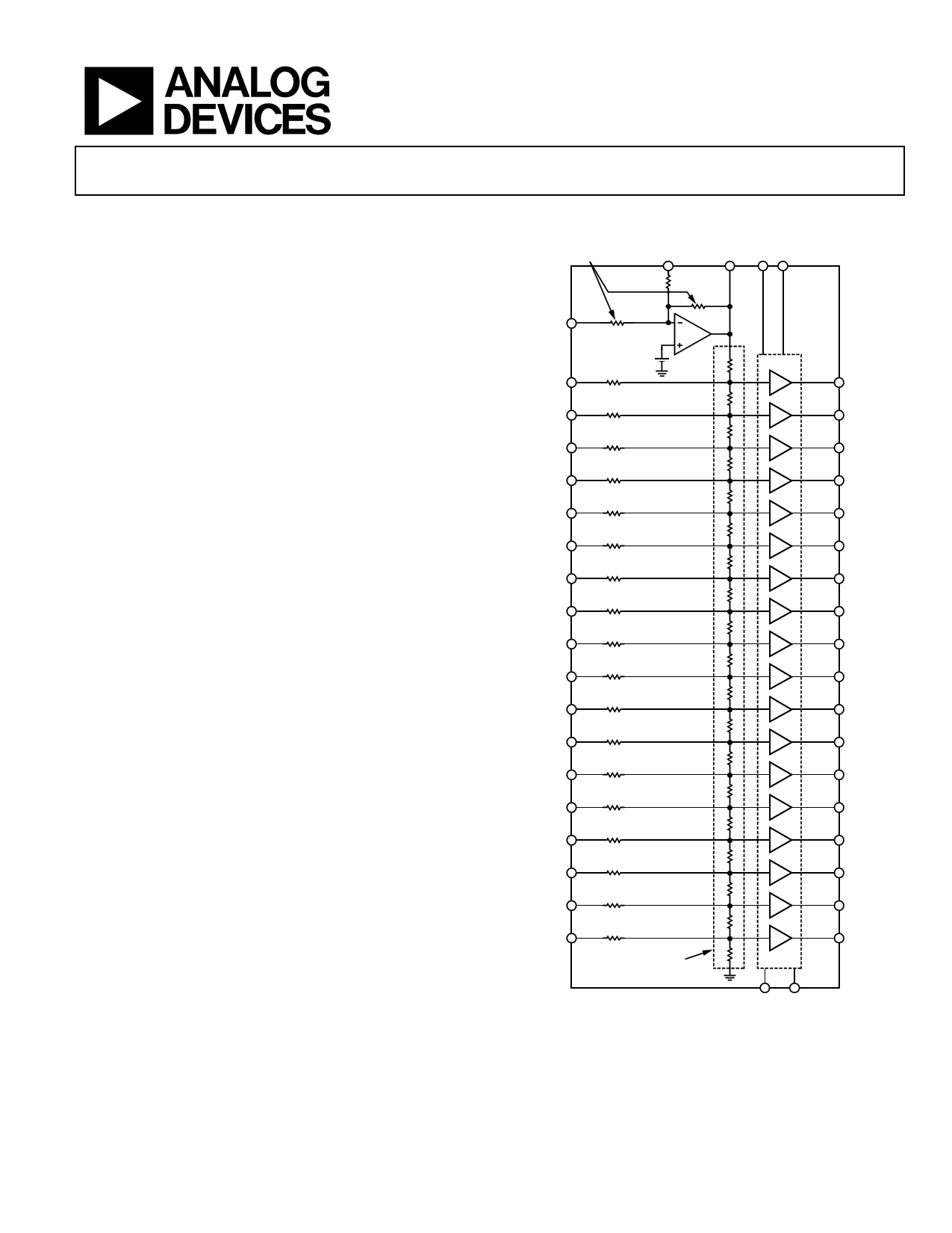
FUNCTIONAL BLOCK DIAGRAM
MASK-PROGRAMMABLE
REGULATOR RESISTORS FB
VREG OUT VDD VDD
700Ω*
GND
VIN18
VIN17
VIN16
VIN15
VIN14
VIN13
VIN12
VIN11
VIN10
VIN9
VIN8
VIN7
VIN6
VIN5
VIN4
VIN3
VIN2
VIN1
+
1.2V –
700Ω*
700Ω*
700Ω*
700Ω*
700Ω*
700Ω*
700Ω*
700Ω*
700Ω*
700Ω*
700Ω*
700Ω*
700Ω*
700Ω*
700Ω*
700Ω*
700Ω*
700Ω*
GAMMA
BUFFERS
VOUT18
VOUT17
VOUT16
VOUT15
VOUT14
VOUT13
VOUT12
VOUT11
VOUT10
VOUT9
VOUT8
VOUT7
VOUT6
VOUT5
VOUT4
VOUT3
VOUT2
VOUT1
MASK-PROGRAMMABLE
RESISTOR STRING
*ESD PROTECTION RESISTORS
GND GND
Figure 1. 48-Lead LQFP or LFCSP
Rev. 0
Information furnished by Analog Devices is believed to be accurate and reliable.
However, no responsibility is assumed by Analog Devices for its use, nor for any
infringements of patents or other rights of third parties that may result from its use.
Specifications subject to change without notice. No license is granted by implication
or otherwise under any patent or patent rights of Analog Devices. Trademarks and
registered trademarks are the property of their respective owners.
One Technology Way, P.O. Box 9106, Norwood, MA 02062-9106, U.S.A.
Tel: 781.329.4700
www.analog.com
Fax: 781.326.8703 © 2004 Analog Devices, Inc. All rights reserved.
1 page 
PIN CONFIGURATION AND FUNCTION DESCRIPTIONS
ADD8708
48 47 46 45 44 43 42 41 40 39 38 37
REGFB 1
GND 2
VDD 3
VREG OUT 4
VIN18 5
VIN17 6
VIN16 7
VIN15 8
VIN14 9
VIN13 10
VIN12 11
VIN11 12
ADD8708
TOP VIEW
(Not to Scale)
36 VOUT10
35 VOUT9
34 VOUT8
33 VOUT7
32 VDD
31 GND
30 VOUT6
29 VOUT5
28 VOUT4
27 VOUT3
26 VOUT2
25 VOUT1
13 14 15 16 17 18 19 20 21 22 23 24
Figure 2. Pin Configuration
Table 4. Pin Function Descriptions
Pin No. Name
Description
1
REGFB
Regulator Feedback. Compares a percentage of the regulator output to the internal 1.2 V voltage
reference. Internal resistors are used to program the desired regulator output voltage.
2 GND Ground. Normally 0 V.
3 VDD
Supply Voltage. Normally 16 V.
4
VREG OUT
Regulator output voltage. Provides reference voltage to resistor string and is internally connected to
the top of the resistor string.
5 VIN18
6 VIN17
7 VIN16
8 VIN15
9 VIN14
10 VIN13
11 VIN12
12 VIN11
13 VIN10
14 VIN9
Buffer inputs. Normally floating.1
15 VIN8
16 VIN7
17 VIN6
18 VIN5
19 VIN4
20 VIN3
21 VIN2
22 VIN1
23 GND
Ground. Normally 0 V.
24 VDD
Supply Voltage. Normally 16 V.
1 External resistors can be added to modify the internal resistor string to change the gamma voltage. An external resistor calculator is available upon request from your
local sales office.
Rev. 0 | Page 5 of 16
5 Page 
VOLTAGE REGULATOR
The on-board voltage regulator provides a regulated voltage to
the resistor chain to provide stable gamma voltages.
The two mask-programmable internal resistors, R1 and R2,
and a reference voltage set the output of the regulator. The
typical values of these parts are shown in Figure 23. In addition,
see the Tap Point and Regulator Voltage Request Form in this
data sheet.
R2
55kΩ
R1
5kΩ
VREF +
1.2V –
VREG OUT
Figure 23. Voltage Regulator
The internal resistors have a typical accuracy of 0.1%. External
resistors can be used to adjust the regulator voltage; however, it
is not recommended. Please contact your local sales office for
further details.
MAXIMUM POWER DISSIPATION
The maximum safe power dissipation in the ADD8708 package
is limited by the associated rise in junction temperature (TJ) on
the die. At approximately 150°C, the glass transition tempera-
ture, the properties of the plastic change. Even temporarily
exceeding this temperature limit may change the stresses that
the package exerts on the die, permanently shifting the para-
metric performance of the ADD8708. Exceeding a junction
temperature of 175°C for an extended period can result in
changes in the silicon devices, potentially causing failure.
ADD8708
LAND PATTERN
The LFCSP package comes with a thermal pad. Soldering down
this thermal pad dramatically improves the heat dissipation of
the package. It is necessary to attach vias that connect the
soldered thermal pad to another layer on the board. This
provides an avenue to dissipate the heat away from the part.
Without vias, the heat is isolated directly under the part.
Subdivide the solder paste, or stencil layer, for the thermal pad
to reduce solder balling and splatter. It is not critical how the
subdivisions are arranged, as long as the total coverage of the
solder paste for the thermal pad is greater than 50%. The land
pattern is critical to heat dissipation. A suggested land pattern is
shown in Figure 22.
The thermal pad is attached to the substrate. In the ADD8708,
the substrate is connected to VDD. To be electrically safe, the
thermal pad should be soldered to an area on the board that is
electrically isolated or connected to VDD. Attaching the thermal
pad to ground adversely affects the performance of the part.
Rev. 0 | Page 11 of 16
11 Page | ||
| Páginas | Total 16 Páginas | |
| PDF Descargar | [ Datasheet ADD8708.PDF ] | |
Hoja de datos destacado
| Número de pieza | Descripción | Fabricantes |
| ADD8701 | 12-Channel Gamma Buffers with VCOM Buffer | Analog Devices |
| ADD8701 | 12-Channel Gamma Buffers with VCOM Buffer | Analog Devices |
| ADD8702 | 12-Channel Gamma Buffers | Analog Devices |
| ADD8704 | 16 V Quad Operational Amplifier | Analog Devices |
| Número de pieza | Descripción | Fabricantes |
| SLA6805M | High Voltage 3 phase Motor Driver IC. |
Sanken |
| SDC1742 | 12- and 14-Bit Hybrid Synchro / Resolver-to-Digital Converters. |
Analog Devices |
|
DataSheet.es es una pagina web que funciona como un repositorio de manuales o hoja de datos de muchos de los productos más populares, |
| DataSheet.es | 2020 | Privacy Policy | Contacto | Buscar |