|
|
|
PDF 8SLVD2104 Data sheet ( Hoja de datos )
| Número de pieza | 8SLVD2104 | |
| Descripción | LVDS Output Fanout Buffer | |
| Fabricantes | IDT | |
| Logotipo | ||
Hay una vista previa y un enlace de descarga de 8SLVD2104 (archivo pdf) en la parte inferior de esta página. Total 16 Páginas | ||
|
No Preview Available !
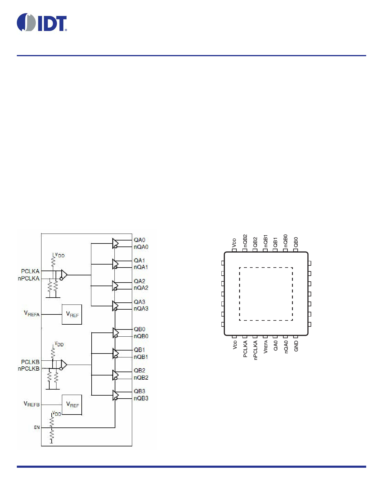
Dual 1:4, LVDS Output Fanout Buffer
8SLVD2104
DATA SHEET
General Description
The 8SLVD2104 is a high-performance differential dual 1:4 LVDS
fanout buffer. The device is designed for the fanout of high-frequency,
very low additive phase-noise clock and data signals. The
8SLVD2104 is characterized to operate from a 2.5V power supply.
Guaranteed output-to-output and part-to-part skew characteristics
make the 8SLVD2104 ideal for those clock distribution applications
demanding well-defined performance and repeatability. Two
independent buffers with four low skew outputs each are available.
The integrated bias voltage generators enables easy interfacing of
single-ended signals to the device inputs. The device is optimized for
low power consumption and low additive phase noise.
Features
• Two 1:4, low skew, low additive jitter LVDS fanout buffers
• Two differential clock inputs
• Differential pairs can accept the following differential input
levels: LVDS and LVPECL
• Maximum input clock frequency: 2GHz
• Output bank skew: 35ps, (maximum)
• Propagation delay: 300ps, (maximum)
• Low additive RMS phase jitter, 156.25MHz (10kHz - 20MHz):
105fs, (maximum)
• 2.5V supply voltage
• Lead-free (RoHS 6) 28-Lead VFQFN package
• -40°C to 85°C ambient operating temperature
Block Diagram
Pin Assignment
28 27 26 25 24 23 22
GND 1
21 nQA3
QB3 2
20 QA3
nQB3 3
EN 4
8SLVD2104 19 nQA2
18 QA2
PCLKB 5
17 nQA1
nPCLKB 6
16 QA1
VREFB 7
15 VDD
8 9 10 11 12 13 14
28-Lead, 5mm x 5mm VFQFN
8SLVD2104 REVISION 1 08/03/15
1 ©2015 Integrated Device Technology, Inc.
1 page 
8SLVD2104 DATA SHEET
Table 4C. Differential Input Characteristics, VDD = 2.5V ± 5%, TA = -40°C to 85°C
Symbol Parameter
Test Conditions
Minimum
Input High PCLKA, nPCLKA
IIH Current PCLKB, nPCLKB
VDD = VIN = 2.625V
Input Low PCLKA, PCLKB
VDD = 2.625V, VIN = 0V
IIL
Current nPCLKA, nPCLKB
VDD = 2.625V, VIN = 0V
VREFA,
VREFB
Reference Voltages
for Input Bias
VDD = 2.5V; IREF = +100µA
VPP
VCMR
Peak-to-Peak Voltage1
Common Mode Input Voltage1, 2
fREF < 1.5 GHz
fREF > 1.5 GHz
NOTE 1: VIL should not be less than -0.3V.
NOTE 2: Common mode input voltage is defined at the crosspoint.
-10
-150
1.0
0.15
0.2
1.0
,
Table 4D. LVDS Output DC Characteristics, VDD = 2.5V ± 5%, TA = -40°C to 85°C1, 2
Symbol Parameter
Test Conditions
Minimum
VOD Differential Output Voltage
VOD
VOD Magnitude Change
VOS Offset Voltage
VOS
VOS Magnitude Change
NOTE 1: Qx, nQx denotes QA[3:0], nQA[3:30], and QB[3:0], nQB[3:0].
NOTE 2: 100 termination across differential outputs.
247
1.0
Typical
Maximum Units
150 µA
µA
µA
1.35 V
1.6
1.6
VDD – VPP/2
V
V
V
Typical
Maximum
454
50
1.4
50
Units
mV
mV
V
mV
REVISION 1 08/03/15
5 DUAL 1:4, LVDS OUTPUT FANOUT BUFFER
5 Page 
8SLVD2104 DATA SHEET
VFQFN EPAD Thermal Release Path
In order to maximize both the removal of heat from the package and
the electrical performance, a land pattern must be incorporated on
the Printed Circuit Board (PCB) within the footprint of the package
corresponding to the exposed metal pad or exposed heat slug on the
package, as shown in Figure 4. The solderable area on the PCB, as
defined by the solder mask, should be at least the same size/shape
as the exposed pad/slug area on the package to maximize the
thermal/electrical performance. Sufficient clearance should be
designed on the PCB between the outer edges of the land pattern
and the inner edges of pad pattern for the leads to avoid any shorts.
While the land pattern on the PCB provides a means of heat transfer
and electrical grounding from the package to the board through a
solder joint, thermal vias are necessary to effectively conduct from
the surface of the PCB to the ground plane(s). The land pattern must
be connected to ground through these vias. The vias act as “heat
pipes”. The number of vias (i.e. “heat pipes”) are application specific
and dependent upon the package power dissipation as well as
electrical conductivity requirements. Thus, thermal and electrical
analysis and/or testing are recommended to determine the minimum
number needed. Maximum thermal and electrical performance is
achieved when an array of vias is incorporated in the land pattern. It
is recommended to use as many vias connected to ground as
possible. It is also recommended that the via diameter should be 12
to 13mils (0.30 to 0.33mm) with 1oz copper via barrel plating. This is
desirable to avoid any solder wicking inside the via during the
soldering process which may result in voids in solder between the
exposed pad/slug and the thermal land. Precautions should be taken
to eliminate any solder voids between the exposed heat slug and the
land pattern. Note: These recommendations are to be used as a
guideline only. For further information, please refer to the Application
Note on the Surface Mount Assembly of Amkor’s Thermally/
Electrically Enhance Leadframe Base Package, Amkor Technology.
PIN SOLDER
EXPOSED HEAT SLUG
SOLDER
PIN
PIN PAD
GROUND PLANE
THERMAL VIA
LAND PATTERN
(GROUND PAD)
PIN PAD
Figure 4. P.C. Assembly for Exposed Pad Thermal Release Path – Side View (drawing not to scale)
REVISION 1 08/03/15
11 DUAL 1:4, LVDS OUTPUT FANOUT BUFFER
11 Page | ||
| Páginas | Total 16 Páginas | |
| PDF Descargar | [ Datasheet 8SLVD2104.PDF ] | |
Hoja de datos destacado
| Número de pieza | Descripción | Fabricantes |
| 8SLVD2102 | LVDS Output Fanout Buffer | IDT |
| 8SLVD2104 | LVDS Output Fanout Buffer | IDT |
| Número de pieza | Descripción | Fabricantes |
| SLA6805M | High Voltage 3 phase Motor Driver IC. |
Sanken |
| SDC1742 | 12- and 14-Bit Hybrid Synchro / Resolver-to-Digital Converters. |
Analog Devices |
|
DataSheet.es es una pagina web que funciona como un repositorio de manuales o hoja de datos de muchos de los productos más populares, |
| DataSheet.es | 2020 | Privacy Policy | Contacto | Buscar |