|
|
|
PDF AWC6325 Data sheet ( Hoja de datos )
| Número de pieza | AWC6325 | |
| Descripción | 3.4V Linear Power Amplifier Module | |
| Fabricantes | Anadigics | |
| Logotipo | ||
Hay una vista previa y un enlace de descarga de AWC6325 (archivo pdf) en la parte inferior de esta página. Total 11 Páginas | ||
|
No Preview Available !
AWC6325
HELP3ETM Dual-band Cellular & PCS CDMA
3.4 V Linear Power Amplifier Module
PRELIMINARY DATA SHEET - Rev 1.4
FEATURES
• InGaP HBT Technology
• High Efficiency:
• 37 % @ POUT = +28 dBm
• 20 % @ POUT = +16 dBm
• 10 % @ POUT = +10 dBm
• Low Quiescent Current: 4 mA
• Internal Voltage Regulation
• Built-in Directional Coupler
• Common VMODE Control Line
• Suitable for SMPS and average power tracking
systems with variable supply voltages
• APT can reduce TS.09 average power
consumption more than 25%
• Reduced External Component Count
• Thin Package: 0.9 mm
• RoHS Compliant Package, 260 oC MSL-3
which greatly reduces the total current drawn from the
battery. This feature, in conjunction with selectable
operating modes, enables significant improvements
in overall power added efficiency of the AWC6325
across the entire dynamic range of operating powers.
APT requires use of an external variable voltage
supply (DC-DC converter), which is used to provide
the variable voltage to Vcc pad of the amplifier. A
low-leakage shutdown mode increases standby time.
This PA has built-in directional couplers for each
band, with a common coupler output port CPL_OUT.
The 3 mm x 5 mm x 0.9 mm surface mount package
incorporates matching networks optimized for output
power, efficiency and linearity in a 50 Ω system. The
device is manufactured on an advanced InGaP HBT
MMIC technology offering state-of-the-art reliability,
temperature stability, and ruggedness.
APPLICATIONS
• Dual-band Wireless Handsets and Data Devices
for CDMA/EVDO networks:
• Cellular BC 0 and 10
• PCS BC 1 and 14
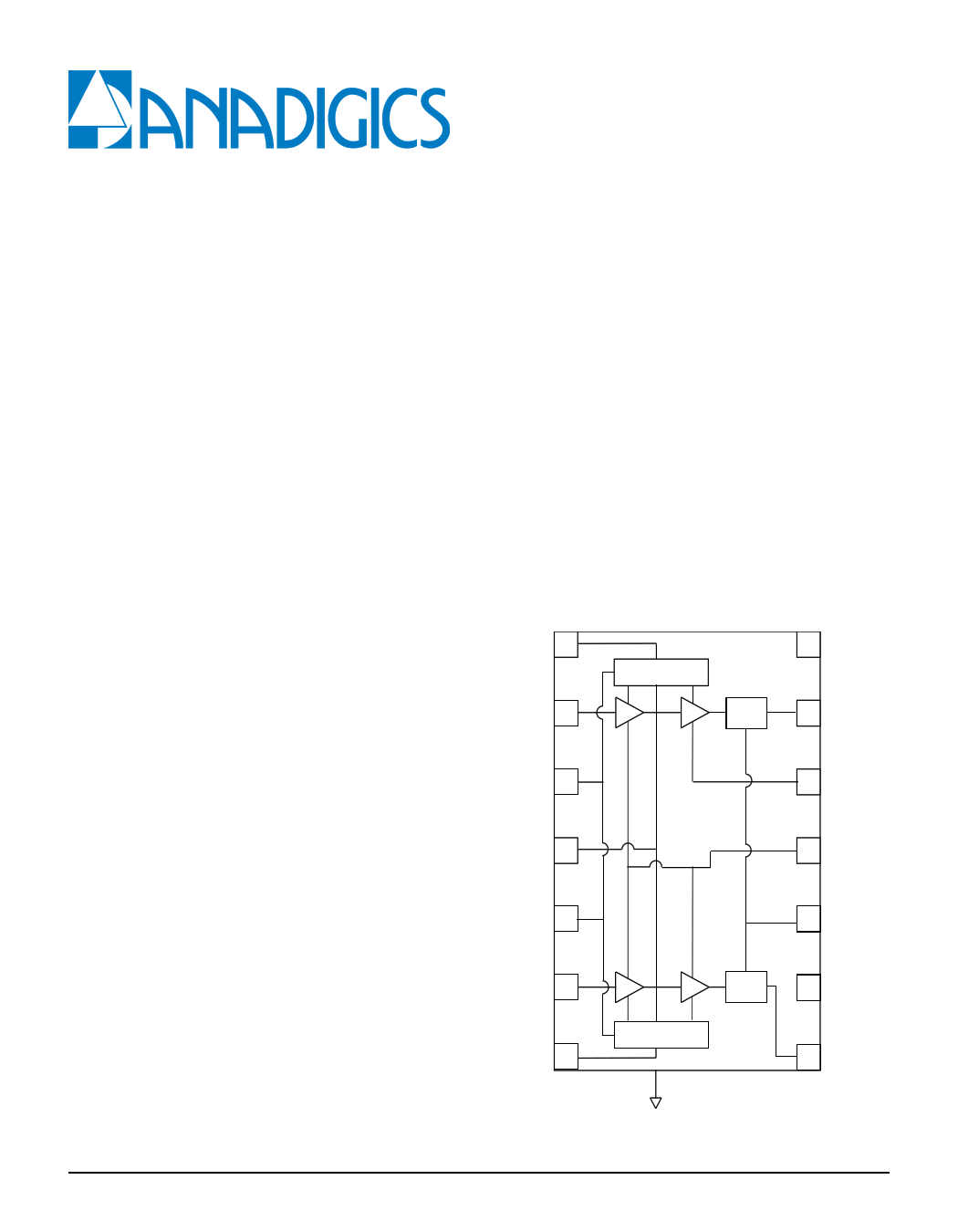
VEN_CELL 1
RFIN_CELL 2
Bias Control
Voltage Regulation
CPL
14 GND
13 RFOUT_CELL
PRODUCT DESCRIPTION
AWC6325 addresses the demand for increased
integration in dual-band handsets for CDMA networks.
The small footprint 3 mm x 5 mm x 0.9 mm surface
mount RoHS compliant package contains independent
RF PA paths to ensure optimal performance in both
frequency bands in less board area than two single
band PAs. The package pinout was chosen to enable
handset manufacturers to independently provide
bias to both power amplifiers and simplify control
with common mode pins. The AWC6325 is part of
ANADIGICS’ 3rd generation of High-Efficiency-at-Low-
Power (HELP3E™) family of power amplifiers, which
deliver low quiescent currents and significantly greater
efficiency through selectable bias modes for high,
medium and low power operation. The AWC6325 is
designed for use both with and without average power
tracking (APT). APT can be used to optimize the Vcc
level for the desired output power level and linearity,
VMODE1 3
VBATT 4
VMODE2 5
RFIN_PCS 6
VEN_PCS 7
01/2014
12 VCC
11 VCCA
10 CPLOUT
CPL 9 GND
Bias Control
Voltage Regulation
8 RFOUT_PCS
GND at Slug (pad)
Figure 1: Block Diagram
1 page 
AWC6325
Table 5: Electrical Specifications - PCS Band (BC 1, 14)
(TC = +25 °C, VBATT = VCC = +3.4 V, VEN_PCS = +1.8 V, 50 Ω system, CDMA2000 RC-1 waveform)
PARAMETER
COMMENTS
MIN TYP MAX UNIT
POUT
VMODE1
VMODE2
24 27 30
+28 dBm 0 V
0V
Gain
10 13 16
dB +16 dBm 1.8 V
0V
6 9 12
+10 dBm 1.8 V
1.8 V
Adjacent Channel Power
at ± 1.25 MHz offset (1)
Primary Channel BW = 1.23 MHz
Adjacent Channel BW = 30 kHz
- -48 -46
- -52.5 -46
- -53 -46
+28 dBm
dBc +16 dBm
+10 dBm
0V
1.8 V
1.8 V
0V
0V
1.8 V
Adjacent Channel Power
at ± 1.98 MHz offset (1)
Primary Channel BW = 1.23 MHz
Adjacent Channel BW = 30 kHz
- -55 -53
+28 dBm 0 V
- -60 -53 dBc +16 dBm 1.8 V
- -63 -53
+10 dBm 1.8 V
0V
0V
1.8 V
Power-Added Efficiency (1)
- 37 -
- 20 -
- 10 -
+28 dBm 0 V
% +16 dBm 1.8 V
+10 dBm 1.8 V
0V
0V
1.8 V
Quiescent Current (Icq)
Mode Control Current
BATT Current
Enable Current
Total Decoder Current on VBATT
(in Shutdown mode)
HBT Leakage Current on VCC
(in Shutdown mode)
Noise In Receive Band
Harmonics
2fO
3fO, 4fO
Input Impedence
Coupling Factor
-4
- 0.5
- 1.5
- 0.3
-8
- <1
- -133
--
--
--
- 22
Spurious Output Level
(all spurious outputs)
--
Load mismatch stress with no
permanent degradation or failure
8:1
Notes:
(1) ACPRs and Efficiency measured at 1880 MHz.
-
- mA through VCC pins, VMODE1,2 = +1.8 V
- mA through VMODE pin, VMODE1,2 = +1.8 V
- mA through VBATT pin, VMODE1,2 = +1.8V
- mA through VEN_PCS pin, VMODE1,2 = +1.8 V
-
µA
VBATT = +4.35 V, VCC = +4.35 V,
VEN_CELL = 0 V, VMODE1,2 = 0 V
-
µA
VBATT = +4.35 V, VCC = +4.35 V,
VEN_CELL = 0 V, VMODE1,2 = 0 V
- dBm/Hz 1930 MHz to 1990 MHz
-30
-30
dBc POUT < +28 dBm
2:1 VSWR
- dB
POUT < +28 dBm
-65
dBc
In-band load VSWR < 5:1
Out-of-band load VSWR < 10:1
Applies over all operating conditions
- VSWR Applies over full operating range
5
PRELIMINARY DATA SHEET - Rev 1.4
01/2014
5 Page 
AWC6325
ORDERING INFORMATION
ORDER NUMBER
TEMPERATURE
RANGE
AWC6325Q7
-30 C to +90 C
AWC6325P9
-30 C to +90 C
PACKAGE
DESCRIPTION
RoHS Compliant 14 Pin
3 mm x 5 mm x 0.9 mm
Surface Mount Module
RoHS Compliant 14 Pin
3 mm x 5 mm x 0.9 mm
Surface Mount Module
COMPONENT PACKAGING
Tape and Reel, 2500 pieces per Reel
Partial Tape and Reel
ANADIGICS, Inc.
141 Mount Bethel Road
Warren, New Jersey 07059, U.S.A.
Tel: +1 (908) 668-5000
Fax: +1 (908) 668-5132
URL: http://www.anadigics.com
IMPORTANT NOTICE
ANADIGICS, Inc. reserves the right to make changes to its products or to discontinue any product at any time without notice.
The product specifications contained in Advanced Product Information sheets and Preliminary Data Sheets are subject to
change prior to a product’s formal introduction. Information in Data Sheets have been carefully checked and are assumed
to be reliable; however, ANADIGICS assumes no responsibilities for inaccuracies. ANADIGICS strongly urges customers
to verify that the information they are using is current before placing orders.
warning
ANADIGICS products are not intended for use in life support appliances, devices or systems. Use of an ANADIGICS product
in any such application without written consent is prohibited.
11
PRELIMINARY DATA SHEET - Rev 1.4
01/2014
11 Page | ||
| Páginas | Total 11 Páginas | |
| PDF Descargar | [ Datasheet AWC6325.PDF ] | |
Hoja de datos destacado
| Número de pieza | Descripción | Fabricantes |
| AWC6323 | HELP3E Dual-band Cellular & PCS CDMA 3.4 V Linear Power Amplifer Module | Anadigics |
| AWC6323 | HELP3E Dual-band Cellular & PCS CDMA 3.4 V Linear Power Amplifer Module | Anadigics |
| AWC6325 | 3.4V Linear Power Amplifier Module | Anadigics |
| Número de pieza | Descripción | Fabricantes |
| SLA6805M | High Voltage 3 phase Motor Driver IC. |
Sanken |
| SDC1742 | 12- and 14-Bit Hybrid Synchro / Resolver-to-Digital Converters. |
Analog Devices |
|
DataSheet.es es una pagina web que funciona como un repositorio de manuales o hoja de datos de muchos de los productos más populares, |
| DataSheet.es | 2020 | Privacy Policy | Contacto | Buscar |