|
|
|
PDF WS2512 Data sheet ( Hoja de datos )
| Número de pieza | WS2512 | |
| Descripción | 4 x 4 Power Amplifier Module | |
| Fabricantes | Agilent | |
| Logotipo | ||
Hay una vista previa y un enlace de descarga de WS2512 (archivo pdf) en la parte inferior de esta página. Total 20 Páginas | ||
|
No Preview Available !
Agilent WS2512
4 x 4 Power Amplifier Module
for UMTS2100 (1920 – 1980 MHz)
Data Sheet
Description
The WS2512, a Wide-band Code
Division Multiple Access
(WCDMA) Power Amplifier (PA),
is a fully matched 10-pin surface
mount module developed for
WCDMA handset applications.
This power amplifier module
operates in the 1920 – 1980 MHz
bandwidth. The WS2512 meets
the stringent WCDMA linearity
requirements for output power of
up to 28 dBm. A low current
(Vcont) pin is provided for high
efficiency improvement of the
low output power range.
The WS2512 features CoolPAM
Circuit technology offering state-
of-the-art reliability, temperature
stability and ruggedness.
The WS2512 is self contained,
incorporating 50ohm input and
output matching networks.
Features
• CoolPAM circuit technology
• Good linearity
• High efficiency
• 10-pin surface mounting package
(4 mm x 4 mm x 1.4 mm)
• Low power-state control
• Low quiescent current
• Internal 50Ω matching networks
for both RF input and output
Applications
• W-CDMA handsets
• HSDPA handsets
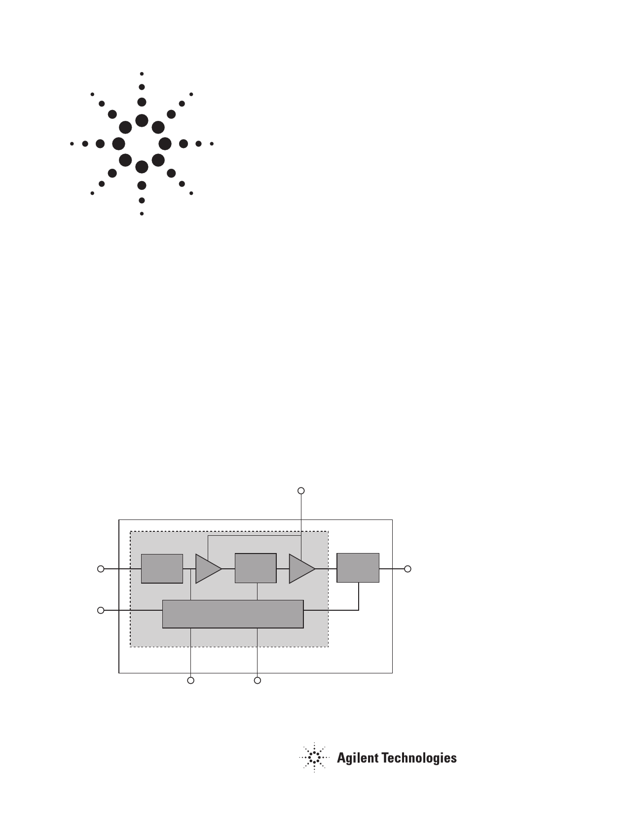
Functional Block Diagram
Vcc2(10)
RF Input (2)
Input
Match
DA
Inter
Stage
Match
PA
Vcc1 (1)
MMIC
Bias Circuit & Control Logic
Vcont(4)
Vref(5)
Output
Match
RF Output (8)
MODULE
1 page 
Characteristics Data (HSDPA, Control scheme: 3-mode control, Vcc = 3.4V, Vref = 2.85V, T = 25°C,
Fo= 1950 MHz)
500
450
400
350
300
250
200
150
100
50
0
-10
-5
0
5 10 15 20 25 30
Pout (dBm)
Figure 1. Total Current vs. Output Power.
30
25
20
15
10
5
0
-10 -5 0 5 10 15 20 25 30
Pout (dBm)
Figure 2. Gain vs. Output Power.
45
40
35
30
25
20
15
10
5
0
-10 -5 0 5 10 15 20 25
Pout (dBm)
Figure 3. Power Added Efficiency vs. Output Power.
30
-30
-35
-40
-45
-50
-55
-60
-10 -5
0
5 10 15 20 25 30
Pout (dBm)
Figure 4. Adjacent Channel Leakage Ratio 1 vs. Output Power.
-40
-45
-50
-55
-60
-65
-70
-10 -5
0
5 10 15 20 25 30
Pout (dBm)
Figure 5. Adjacent Channel Leakage Ratio 2 vs. Output Power.
5
5 Page 
Peripheral Circuit in Handset
V BATT
5
RF In
RF SAW
C2
Vdd
C3
C1
MSM
PA_R0
PA_ON
R1
+2.85V
Figure 21. Peripheral Circuit.
Vcc1
IN
GND
Vcont
Vref
Vcc2
GND
OUT
GND
GND
WS2512
C4
C6 RF Out
Duplexer
C7 L1
Output Matching Circuit
C8
Notes:
1. Recommended voltage for Vref is 2.85V.
2. Place C1 near to Vref pin.
3. Place C3 and C4 close to pin 1 (Vcc1) and pin 10 (Vcc2). These capacitors can affect the RF performance.
4. Use 50Ω transmission line between PAM and Duplexer and make it as short as possible to reduce conduction loss.
5. π-type circuit topology is good to use for matching circuit between PA and Duplexer.
6. Pull-up resistor (R1) should be used to limit current drain. 6.2 kohm is recommended for WS2512.
11
11 Page | ||
| Páginas | Total 20 Páginas | |
| PDF Descargar | [ Datasheet WS2512.PDF ] | |
Hoja de datos destacado
| Número de pieza | Descripción | Fabricantes |
| WS2512 | 4 x 4 Power Amplifier Module | Agilent |
| WS2512-TR1G | 4 x 4 Power Amplifier Module | Avago |
| Número de pieza | Descripción | Fabricantes |
| SLA6805M | High Voltage 3 phase Motor Driver IC. |
Sanken |
| SDC1742 | 12- and 14-Bit Hybrid Synchro / Resolver-to-Digital Converters. |
Analog Devices |
|
DataSheet.es es una pagina web que funciona como un repositorio de manuales o hoja de datos de muchos de los productos más populares, |
| DataSheet.es | 2020 | Privacy Policy | Contacto | Buscar |