|
|
|
PDF ADRF6510 Data sheet ( Hoja de datos )
| Número de pieza | ADRF6510 | |
| Descripción | 30 MHz Dual Programmable Filters and Variable Gain Amplifiers | |
| Fabricantes | Analog Devices | |
| Logotipo | ||
Hay una vista previa y un enlace de descarga de ADRF6510 (archivo pdf) en la parte inferior de esta página. Total 28 Páginas | ||
|
No Preview Available !
30 MHz Dual Programmable Filterswww.DataSheet4U.com
and Variable Gain Amplifiers
ADRF6510
FEATURES
Matched pair of programmable filters and VGAs
Continuous gain control range: −5 dB to +45 dB
6-pole filter
1 MHz to 30 MHz in 1 MHz steps, 0.5 dB corner frequency
SPI programmable
6 dB front-end gain step
IMD3: >55 dBc for 1.5 V p-p composite output
HD2, HD3: >60 dBc for 1.5 V p-p output
Differential input and output
Adjustable output common-mode voltage
Optional dc output offset correction
Power-down feature
Single 5 V supply operation
APPLICATIONS
Baseband I/Q receivers
Diversity receivers
ADC drivers
GENERAL DESCRIPTION
The ADRF6510 is a matched pair of fully differential low noise
and low distortion programmable filters and variable gain ampli-
fiers (VGAs). Each channel is capable of rejecting large out-of-
band interferers while reliably boosting the wanted signal, thus
reducing the bandwidth and resolution requirements on the
analog-to-digital converters (ADCs). The excellent matching
between channels and their high spurious-free dynamic range
over all gain and bandwidth settings make the ADRF6510 ideal
for quadrature-based (IQ) communication systems with dense
constellations, multiple carriers, and nearby interferers.
The filters provide a six-pole Butterworth response with 0.5 dB
corner frequencies programmable through the SPI port from
1 MHz to 30 MHz in 1 MHz steps. The preamplifier that precedes
the filters offers a pin-programmable option of either 6 dB or
12 dB of gain. The preamplifier sets a differential input imped-
ance of 400 Ω and has a common-mode voltage that defaults
to 2.1 V but can be driven from 1.5 V to 2.5 V.
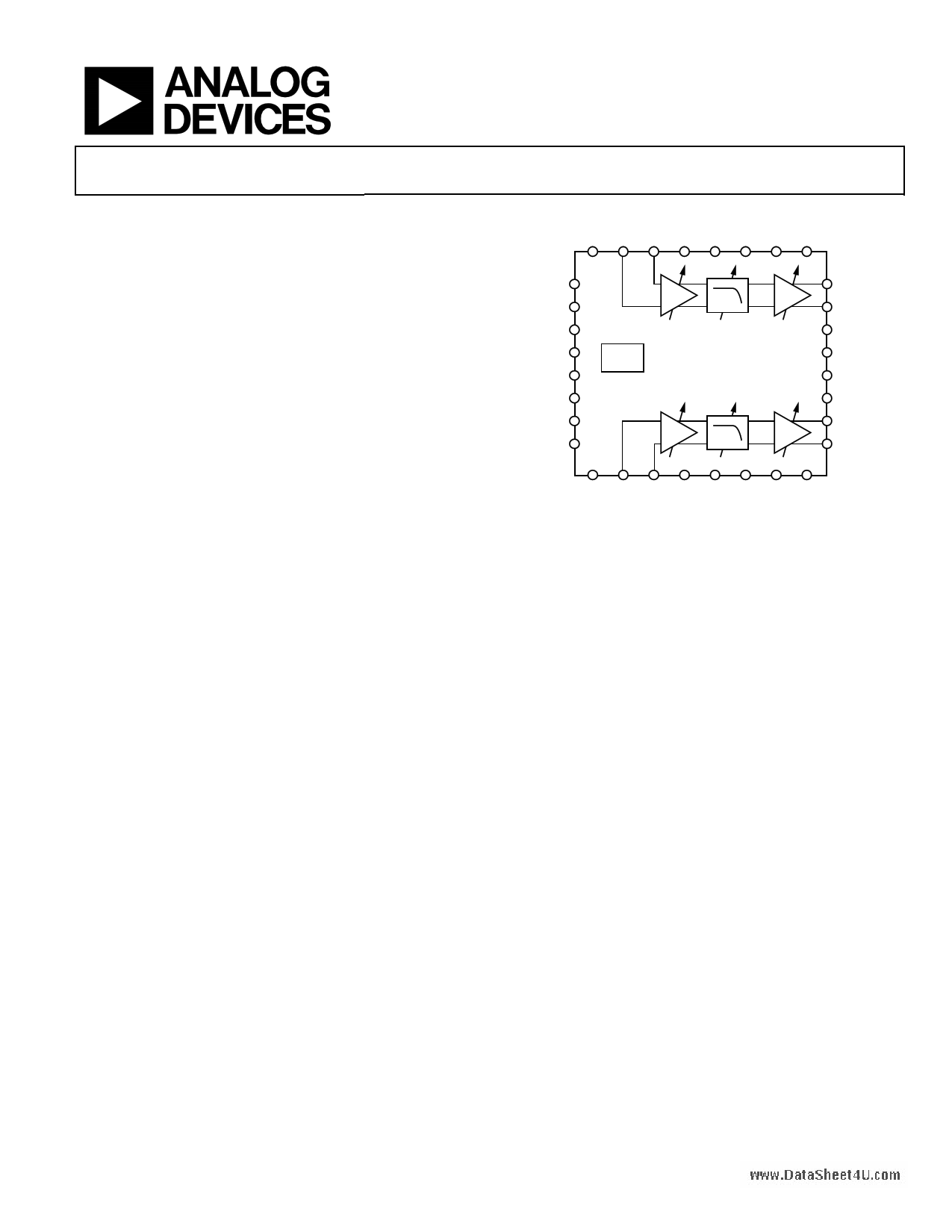
FUNCTIONAL BLOCK DIAGRAM
ENBL INP1 INM1 VPS COM GNSW OFS1 VPS
VPSD
COMD
LE
CLK
DATA
SDO
COM
VPS
SPI ADRF6510
OPP1
OPM1
COM
GAIN
VOCM
COM
OPM2
OPP2
COM INP2 INM2 VPS COM OFDS OFS2 VPS
Figure 1.
The variable gain amplifiers that follow the filters provide 50 dB
of continuous gain control with a slope of 30 mV/dB. The output
buffers provide a differential output impedance of 20 Ω that is
capable of driving 1.5 V p-p into 1 kΩ loads. The output common-
mode voltage defaults to VPS/2, but it can be programmed via the
VOCM pin. The built-in dc offset correction loop can be disabled
if dc-coupled operation is desired. The high-pass corner frequency
is defined by external capacitors on the OFS1 and OFS2 pins.
The ADRF6510 operates from a 4.75 V to 5.25 V supply and
consumes a maximum supply current of 258 mA when pro-
grammed to the highest bandwidth setting. When disabled, it
consumes 2 mA. The ADRF6510 is fabricated in an advanced
silicon-germanium BiCMOS process and is available in a
32-lead, exposed paddle LFCSP. Performance is specified over
the −40°C to +85°C temperature range.
Rev. 0
Information furnished by Analog Devices is believed to be accurate and reliable. However, no
responsibility is assumed by Analog Devices for its use, nor for any infringements of patents or other
rights of third parties that may result from its use. Specifications subject to change without notice. No
license is granted by implication or otherwise under any patent or patent rights of Analog Devices.
Trademarksandregisteredtrademarksarethepropertyoftheirrespectiveowners.
One Technology Way, P.O. Box 9106, Norwood, MA 02062-9106, U.S.A.
Tel: 781.329.4700
www.analog.com
Fax: 781.461.3113
©2010 Analog Devices, Inc. All rights reserved.
1 page 
TIMING DIAGRAMS
ADRF6510www.DataSheet4U.com
tCLK
tPW
CLK
LE
DATA
tLS
tDS tDH
WRITE BIT
LSB
LSB + 1
MSB – 2
MSB – 1
MMSSBB- 2
tLH
NOTES
1. THE FIRST DATA BIT DETERMINES WHETHER THE PART IS WRITING TO OR READING FROM THE INTERNAL CORNER FREQUENCY
WORD REGISTER. FOR A WRITE OPERATION, THE FIRST BIT SHOULD BE A LOGIC 1. THE CORNER FREQUENCY WORD BIT IS THEN
REGISTERED INTO THE DATA PIN ON CONSECUTIVE RISING EDGES OF THE CLOCK.
Figure 2. Write Mode Timing Diagram
CLK
tD
tLS
tCLK
tPW
tLH
LE
tDS tDH
DATA
READ BIT
DC
DC
DC DC
DC
DC
DC
SDO
LSB
LSB + 1
MSB – 2
MSB – 1
MSB
NOTES
1. THE FIRST DATA BIT DETERMINES WHETHER THE PART IS WRITING TO OR READING FROM THE INTERNAL CORNER FREQUENCY WORD
REGISTER. FOR A READ OPERATION, THE FIRST BIT SHOULD BE A LOGIC 0. THE CORNER FREQUENCY WORD BIT IS THEN UPDATED AT
THE SDO PIN ON CONSECUTIVE FALLING EDGES OF THE CLOCK.
Figure 3. Read Mode Timing Diagram
Rev. 0 | Page 5 of 28
5 Page 
30
BANDWIDTH = 30MHz
f1 = 14MHz, f2 = 15MHz
25
+25°C
20
+85°C
15
–40°C
10
5
0
0 5 10 15 20 25 30 35
GAIN (dB)
Figure 23. In-Band OIP3 vs. Gain over Temperature
(Preamp Gain = 6 dB, Bandwidth Setting = 30 MHz)
40
120
GAIN = 0dB
GAIN = 10dB
100 GAIN = 20dB
GAIN = 30dB
GAIN = 40dB
80
60
40
20
0
0 0.5 1.0 1.5 2.0 2.5 3.0 3.5 4.0
COMPOSITE OUTPUT VOLTAGE (V p-p)
Figure 24. In-Band Third-Order Intermodulation Distortion
(Preamp Gain = 6 dB, Bandwidth Setting = 30 MHz)
120
GAIN = 6dB
GAIN = 16dB
100 GAIN = 26dB
GAIN = 36dB
GAIN = 46dB
80
60
40
20
0
0 0.5 1.0 1.5 2.0 2.5 3.0 3.5 4.0
COMPOSITE OUTPUT VOLTAGE (V p-p)
Figure 25. In-Band Third-Order Intermodulation Distortion
(Preamp Gain = 12 dB, Bandwidth Setting = 30 MHz)
ADRF6510www.DataSheet4U.com
65
55 BANDWIDTH = 30MHz
45
35
25
15
5
–5
–15 2:1 SLOPE
–25
–35
–45 PREAMP
–55 GAIN = 12dB
–65 OUT-OF-BAND IIP2
–75
–85
–95
–105
–115
PREAMP
GAIN = 6dB
–125
–135
–145
–45 –35 –25 –15 –5 5 15 25 35 45 55
INPUT LEVEL @ 115MHz AND 130MHz (dBV/Tone)
Figure 26. Out-of-Band IIP2: IMD2 Tone at Midband
(Bandwidth Setting = 30 MHz)
65
10
0 BANDWIDTH = 30MHz
–10
–20
–30
–40 3:1 SLOPE
–50
–60
PREAMP
–70 GAIN = 12dB
–80
OUT-OF-BAND IIP3
–90
–100
–110
PREAMP
GAIN = 6dB
–120
–130
–45
–40 –35 –30 –25 –20 –15 –10 –5 0
INPUT LEVEL @ 115MHz AND 215MHz (dBV/Tone)
Figure 27. Out-of-Band IIP3: IMD3 Tone at Midband
(Bandwidth Setting = 30 MHz)
5
70
65 1MHz BW
2MHz BW
60
4MHz BW
6MHz BW
55 8MHz BW
30MHz BW
50
45
40
35
30
25
20
–5 0 5 10 15 20 25 30 35 40 45
GAIN (dB)
Figure 28. Noise Figure vs. Gain over Bandwidth Setting,
Preamp Gain = 6 dB (Noise Figure at 1/2 Bandwidth)
Rev. 0 | Page 11 of 28
11 Page | ||
| Páginas | Total 28 Páginas | |
| PDF Descargar | [ Datasheet ADRF6510.PDF ] | |
Hoja de datos destacado
| Número de pieza | Descripción | Fabricantes |
| ADRF6510 | 30 MHz Dual Programmable Filters and Variable Gain Amplifiers | Analog Devices |
| ADRF6516 | Dual Programmable Filters | Analog Devices |
| ADRF6518 | Dual Programmable Filters and Variable Gain Amplifiers | Analog Devices |
| Número de pieza | Descripción | Fabricantes |
| SLA6805M | High Voltage 3 phase Motor Driver IC. |
Sanken |
| SDC1742 | 12- and 14-Bit Hybrid Synchro / Resolver-to-Digital Converters. |
Analog Devices |
|
DataSheet.es es una pagina web que funciona como un repositorio de manuales o hoja de datos de muchos de los productos más populares, |
| DataSheet.es | 2020 | Privacy Policy | Contacto | Buscar |