|
|
|
PDF MW4IC2020GMBR1 Data sheet ( Hoja de datos )
| Número de pieza | MW4IC2020GMBR1 | |
| Descripción | RF LDMOS Wideband Integrated Power Amplifiers | |
| Fabricantes | Motorola Semiconductors | |
| Logotipo | ||
Hay una vista previa y un enlace de descarga de MW4IC2020GMBR1 (archivo pdf) en la parte inferior de esta página. Total 12 Páginas | ||
|
No Preview Available !
www.DataSheet4U.com
MOTOROLA
Freescale Semiconductor, Inc.
SEMICONDUCTOR TECHNICAL DATA
Order this document
by MW4IC2020/D
The Wideband IC Line
RF LDMOS Wideband Integrated
Power Amplifiers
MW4IC2020MBR1
MW4IC2020GMBR1
The MW4IC2020M wideband integrated circuit is designed for base station
applications. It uses Motorola’s newest High Voltage (26 to 28 Volts) LDMOS IC
technology and integrates a multi - stage structure. Its wideband On - Chip
design makes it usable from 1600 to 2400 MHz. The linearity performances
cover all modulations for cellular applications: GSM, GSM EDGE, TDMA,
CDMA and W - CDMA.
Final Application
Typical Two - Tone Performance: VDD = 26 Volts, IDQ1 = 80 mA, IDQ2 =
200 mA, IDQ3 = 300 mA, Pout = 20 Watts PEP, Full Frequency Band
Power Gain — 29 dB
IMD — - 32 dBc
Drain Efficiency — 26% (at 1805 MHz) and 20% (at 1990 MHz)
Driver Applications
Typical GSM EDGE Performance: VDD = 26 Volts, IDQ1 = 80 mA, IDQ2 =
230 mA, IDQ3 = 230 mA, Pout = 5 Watts Avg., Full Frequency Band
Power Gain — 29 dB
Spectral Regrowth @ 400 kHz Offset = - 66 dBc
Spectral Regrowth @ 600 kHz Offset = - 77 dBc
EVM — 1% rms
Typical CDMA Performance: VDD = 26 Volts, IDQ1 = 80 mA, IDQ2 =
240 mA, IDQ3 = 250 mA, Pout = 1 Watt Avg., Full Frequency Band, IS - 97
Pilot, Sync, Paging, Traffic Codes 8 through 13
Power Gain — 30 dB
ACPR @ 885 kHz Offset = - 61 dBc @ 30 kHz Bandwidth
ALT1 @ 1.25 MHz Offset = - 69 dBc @ 12.5 kHz Bandwidth
ALT2 @ 2.25 MHz Offset = - 59 dBc @ 1 MHz Bandwidth
• Capable of Handling 3:1 VSWR, @ 26 Vdc, 1990 MHz, 8 Watts CW
Output Power
• Characterized with Series Equivalent Large - Signal Impedance Parameters
• On - Chip Matching (50 Ohm Input, DC Blocked, >5 Ohm Output)
• Integrated Temperature Compensation with Enable/Disable Function
• On - Chip Current Mirror gm Reference FET for Self Biasing Application (1)
• Integrated ESD Protection
• Also Available in Gull Wing for Surface Mount
• In Tape and Reel. R1 Suffix = 500 Units per 44 mm, 13 inch Reel
1805 - 1990 MHz, 20 W, 26 V
GSM/GSM EDGE, CDMA
RF LDMOS WIDEBAND
INTEGRATED POWER AMPLIFIERS
CASE 1329 - 09
TO - 272 WB - 16
PLASTIC
MW4IC2020MBR1
CASE 1329A - 03
TO - 272 WB - 16 GULL
PLASTIC
MW4IC2020GMBR1
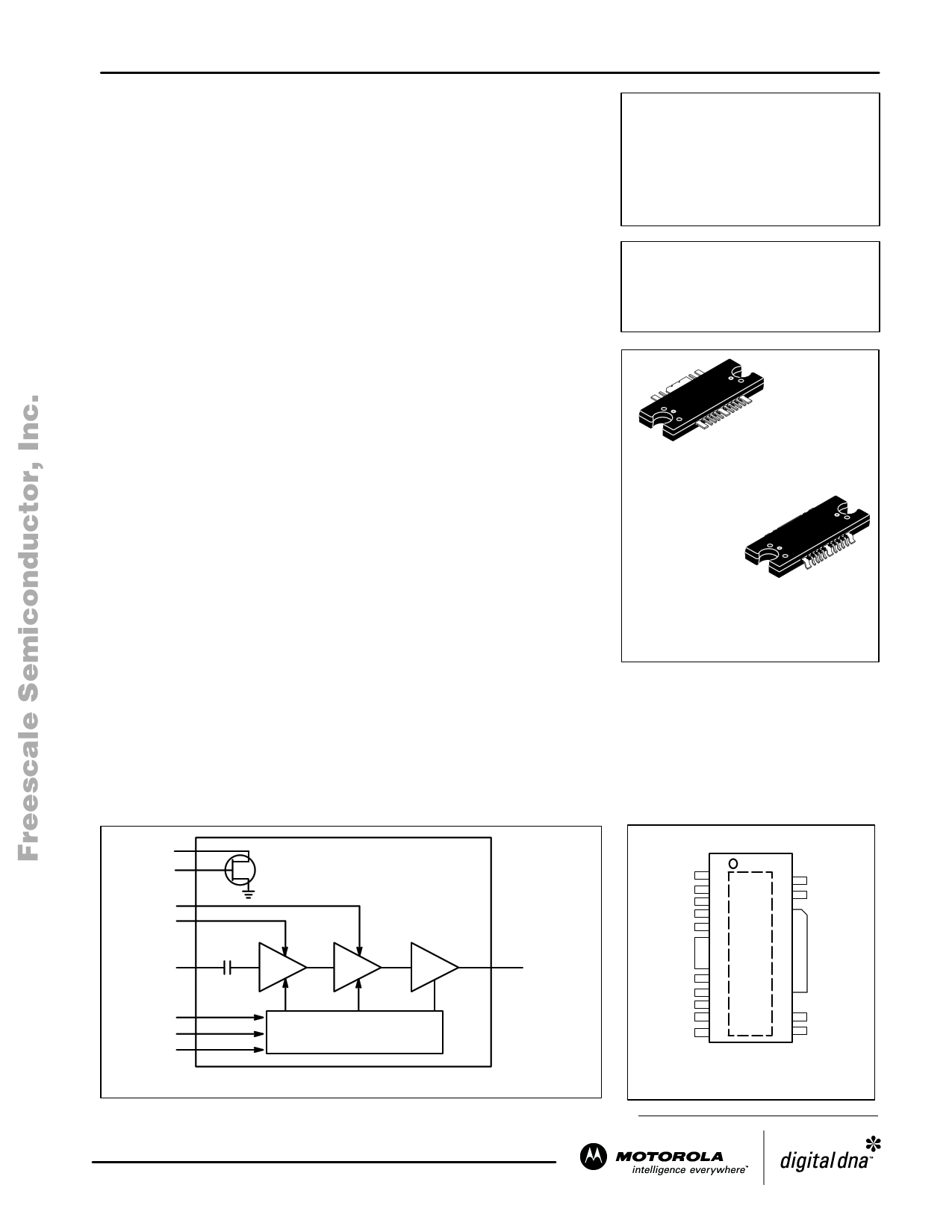
PIN CONNECTIONS
VRD1
VRG1
VDS2
VDS1
RFin
VGS1
VGS2
VGS3
3 Stages IC
Quiescent Current
Temperature Compensation
VDS3/RFout
GND
VDS2
VRD1
VRG1
VDS1
RFin
VGS1
VGS2
VGS3
GND
1
2
3
16
15
4
5
6 14
7
8
9
10 13
11 12
(Top View)
GND
VDS3/
RFout
GND
Functional Block Diagram
NOTE: Exposed backside flag is source
terminal for transistors.
(1) Refer to AN1987/D, Quiescent Current Control for the RF Integrated Circuit Device Family. Go to http://www.motorola.com/semiconductors/rf .
Select Documentation/Application Notes - AN1987.
REV 4
MMoOtorToOla,RInOc.L2A00R4 F DEVICE DATA
MW4IC2020MBR1 MW4IC2020GMBR1
For More Information On This Product,
Go to: www.freescale.com
1
1 page 
www.DataSheet4U.com
Freescale Semiconductor, Inc.
C2
VD2
VD1
C1
MW4IC2020
Rev 1
C5
C6
C7
VG1 R1
R2
VG2
C4
R3
VG3
C3
C8 VD3
C9
C10 C11 C12 C13
C14
GND
Figure 2. MW4IC2020MBR1(GMBR1) Test Circuit Component Layout
MOTOROLA RF DEVICE DATA
MW4IC2020MBR1 MW4IC2020GMBR1
For More Information On This Product,
Go to: www.freescale.com
5
5 Page 
www.DataSheet4U.com
2X r1
aaa M C A B
PIN ONE
INDEX
6X
e1
4X
e2
e
D1
b2
aaa M C A
Freescale Semiconductor, Inc.
E1 B
A
4X b1
aaa M C A
2X
e3
b3
aaa M C A D M
10X b
aaa M C A
ÉÉÉÉÉÉÉÉÉÉÉÉÉÉÉÉÉÉÉÉÉÉÉÉÉÉÉÉÉÉÉÉÉÉÉÉÉÉÉÉÉÉÉÉÉÉÉÉÉÉÉÉÉÉÉÉÉÉÉÉÉÉÉÉÉÉÉÉÉÉÉÉ NOTE6
DATUM
PLANE
H
c1
tL
E
DETAIL Y
A A2
E2
YY
C
SEATING
PLANE
DETAIL Y
L1
GAGE
PLANE
A1
NOTES:
1. CONTROLLING DIMENSION: INCH.
2. INTERPRET DIMENSIONS AND TOLERANCES PER
ASME Y14.5M−1994.
3. DATUM PLANE −H− IS LOCATED AT TOP OF LEAD
AND IS COINCIDENT WITH THE LEAD WHERE THE
LEAD EXITS THE PLASTIC BODY AT THE TOP OF
THE PARTING LINE.
4. DIMENSIONS "D" AND "E1" DO NOT INCLUDE
MOLD PROTRUSION. ALLOWABLE PROTRUSION
IS .006 (0.15) PER SIDE. DIMENSIONS "D" AND "E1"
DO INCLUDE MOLD MISMATCH AND ARE
DETERMINED AT DATUM PLANE −H−.
5. DIMENSIONS "b", "b1", "b2" AND "b3" DO NOT
INCLUDE DAMBAR PROTRUSION. ALLOWABLE
DAMBAR PROTRUSION SHALL BE .005 (0.13)
TOTAL IN EXCESS OF THE "b", "b1", "b2" AND "b3"
DIMENSIONS AT MAXIMUM MATERIAL CONDITION.
6. HATCHING REPRESENTS THE EXPOSED AREA OF
THE HEAT SINK.
CASE 1329A - 03
ISSUE B
TO - 272 WB - 16 GULL
PLASTIC
MW4IC2020GMBR1
N
E2
VIEW Y - Y
INCHES
MILLIMETERS
DIM MIN MAX MIN MAX
A .100 .104 2.54 2.64
A1 .001 .004 0.02 0.10
A2 .099 .110 2.51 2.79
D .928 .932 23.57 23.67
D1 .810 BSC
20.57 BSC
E .429 .437 10.90 11.10
E1 .353 .357 8.97 9.07
E2 .346 .350 8.79 8.89
L .018 .024 4.90 5.06
L1 .01 BSC
0.25 BSC
M .600 −−− 15.24 −−−
N .270 −−− 6.86 −−−
b .011 .017 0.28 0.43
b1 .037 .043 0.94 1.09
b2 .037 .043 0.94 1.09
b3 .225 .231 5.72 5.87
c1 .007 .011 .18 .28
e .054 BSC
1.37 BSC
e1 .040 BSC
1.02 BSC
e2 .224 BSC
5.69 BSC
e3 .150 BSC
3.81 BSC
r1 .063 .068
t 2° 8 °
1.6 1.73
2° 8°
aaa .004
.10
MOTOROLA RF DEVICE DATA
MW4IC2020MBR1 MW4IC2020GMBR1
For More Information On This Product,
Go to: www.freescale.com
11
11 Page | ||
| Páginas | Total 12 Páginas | |
| PDF Descargar | [ Datasheet MW4IC2020GMBR1.PDF ] | |
Hoja de datos destacado
| Número de pieza | Descripción | Fabricantes |
| MW4IC2020GMBR1 | RF LDMOS Wideband Integrated Power Amplifiers | Motorola Semiconductors |
| Número de pieza | Descripción | Fabricantes |
| SLA6805M | High Voltage 3 phase Motor Driver IC. |
Sanken |
| SDC1742 | 12- and 14-Bit Hybrid Synchro / Resolver-to-Digital Converters. |
Analog Devices |
|
DataSheet.es es una pagina web que funciona como un repositorio de manuales o hoja de datos de muchos de los productos más populares, |
| DataSheet.es | 2020 | Privacy Policy | Contacto | Buscar |