OPA2607 반도체 회로 부품 판매점
Dual / High Output / Current-Feedback OPERATIONAL AMPLIFIER
|
|
|
Burr-Brown |
®
OPA2607
OPA2607
For most current data sheet and other product
information, visit www.burr-brown.com
OPA2607
TM Dual, High Output, Current-Feedback
OPERATIONAL AMPLIFIER
FEATURES
q WIDEBAND ±12V OPERATION: 25MHz (G = +8)
q UNITY GAIN STABLE: 35MHz (G = +1)
q HIGH OUTPUT CURRENT: 250mA
q OUTPUT VOLTAGE SWING: ±10.5V (VS = ±12V)
q HIGH SLEW RATE: 600V/µs
q LOW SUPPLY CURRENT: 8mA/channel
q FLEXIBLE POWER CONTROL (SO-14)
q ±6V TO ±16V SUPPLY RANGE
q POWER PACKAGING
APPLICATIONS
q xDSL LINE DRIVER
q LOW-NOISE ADSL RECEIVER
q LOW-COST VIDEO DA
q LOW-COST UPGRADE TO LT1207/AD812
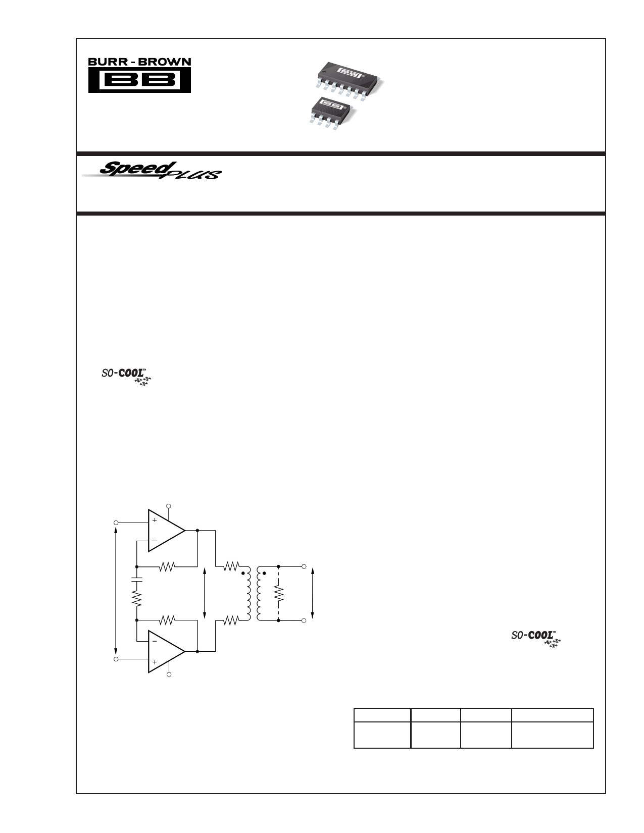
4.8Vp-p
+12V
1/2
OPA2607
1.21kΩ
100nF
348Ω
1.21kΩ
78.7Ω 1:0.8
38Vp-p
78.7Ω
100Ω 15Vp-p
1/2
OPA2607
–12V
Low Turns Ratio ADSL Upstream Driver
DESCRIPTION
The OPA2607 provides a high output voltage swing and low
distortion required for low turns ratio ADSL upstream driver
applications. Operating on a ±12V supply, the OPA2607 con-
sumes a low 8.0mA/channel quiescent current to deliver a very
high 250mA peak output current. Guaranteed output current of
180mA supports even the most demanding ADSL CPE require-
ments with low harmonic distortion. Differential driver applica-
tions will deliver < –75dBc distortion at the peak upstream power
levels of full rate ADSL. Using a differential driver design, as
shown below, the OPA2607 can deliver a high 38Vp-p voltage
swing into a 1:0.8 step-down transformer to meet the ADSL CPE
upstream power requirements. This low turns ratio actually pro-
vides a step up to the much weaker downstream signal arriving on
the line side of this transformer, extending the DSL modem’s
reach.
Power control features are included in the SO-14 package version
to allow system power to be minimized. Two logic control lines
allow four quiescent power settings. These include full power,
power cutback for short loops, idle state for no signal transmission
but line match maintenance, and shutdown for power off with a
high impedance output. An additional IADJ pin allows the maxi-
mum supply current to be adjusted ±25% from the nominal value.
Connecting this pin to +VCC will increase the full power quiescent
to 20mA, increasing the peak output current available, while
connecting this pin to –VCC will decrease the full power quiescent
to 12mA where a lower peak output current is required. The
digital control lines continue to scale the total quiescent current
from these new maximum levels in the same proportional steps as
before.
The OPA2607 is available in three package styles. For power
driver applications, a thermally enhanced
package
with a heat slug is available in both SO-8 and SO-14 pinouts. For
lower power receiver applications, a standard SO-8 package is
available.
OPA2607 RELATED PRODUCTS
SINGLES
DUALS
TRIPLES
NOTES
OPA681
—
OPA2681
OPA2677
OPA3681
—
Single +12V Capable
Single +12V Capable
SBOS128
International Airport Industrial Park • Mailing Address: PO Box 11400, Tucson, AZ 85734 • Street Address: 6730 S. Tucson Blvd., Tucson, AZ 85706 • Tel: (520) 746-1111
Twx: 910-952-1111 • Internet: http://www.burr-brown.com/ • Cable: BBRCORP • Telex: 066-6491 • FAX: (520) 889-1510 • Immediate Product Info: (800) 548-6132
©2000 Burr-Brown Corporation
PDS-11615A
OPPArin2te6d i0n 7U.S.A. August, 2000
®

SPECIFICATIONS: VS = ±12V
RF = 1.21kΩ, RL = 100Ω, and G = +8, unless otherwise noted.
OPA2607H, U, N
PARAMETER
CONDITIONS
TYP
+25°C
+25°C(2)
GUARANTEED
0°C to
70°C(3)
–40°C to
+85°C(3)
UNITS
MIN/ TEST
MAX LEVEL(1)
AC PERFORMANCE (see Figure 1)
Small-Signal Bandwidth (VO = 0.5Vp-p)
Bandwidth for 0.1dB Gain Flatness
Large-Signal Bandwidth
Slew Rate
Rise/Fall Time
Spurious Free Dynamic Range(4)
Input Voltage Noise
Non-Inverting Input Current Noise
Inverting Input Current Noise
Differential Gain
Differential Phase
Channel-to-Channel Crosstalk
G = +1, RF = 1.50kΩ
G = +2, RF = 1.43kΩ
G = +4, RF = 1.37kΩ
G = +8, RF = 1.21kΩ
G = +8, VO = 0.5Vp-p
G = +8, VO = 20Vp-p
G = +8, VO = 20V Step
G = +8, VO = 0.5V Step
VO = 2Vp-p, 1MHz, RL = 100Ω
VO = 20Vp-p, 150kHz, RL = 150Ω
NTSC, G = +2, RL = 150Ω
NTSC, G = +2, RL = 150Ω
f = 1MHz
35
28
25
25
6
13
600
14
77
75
1.7
11
15
0.01
0.01
–60
19
10.6
470
18
66
70
2.0
13
17
18
9.0
400
20
60
58
2.6
13
17
MHz typ C
MHz typ C
MHz typ C
17 MHz min B
MHz typ C
7.9 MHz min B
350 V/µs min B
21 ns min B
57 dB min B
57 dB min B
2.7 nV/√Hz max B
13 pA/√Hz max B
17 pA/√Hz max B
% typ C
degrees typ C
dB typ C
DC PERFORMANCE(5)
Open-Loop Transimpedance Gain
Input Offset Voltage
Average Offset Voltage Drift
Non-Inverting Input Bias Current
Average Non-Inverting Input Bias Current Drift
Inverting Input Bias Current
Average Inverting Input Bias Current Drift
INPUT
Common-Mode Input Range (CMIR)
Common-Mode Rejection Ratio (CMRR)
Non-Inverting Input Impedance
Inverting Input Resistance
VO = 0V, RL = 100Ω
VCM = 0V
VCM = 0V
VCM = 0V
VCM = 0V
VCM = 0V
VCM = 0V
VCM = 0V
Open-Loop
950
±1.5
±3
±4
440
±7
±12
±40
±10.3
64
250 || 4
33
±10.0
53
390
±8
–20
±15
–70
±58
–380
±9.9
52
310
±8.5
–25
±20
–100
±70
–425
kΩ min A
mV max A
µV/°C max B
µA max A
nA/°C max B
µA max A
nA/°C max B
±9.8
51
V
dB
kΩ || pF
Ω
min
min
typ
typ
A
A
C
C
OUTPUT
Voltage Output Swing
Current Output, Sourcing
Current Output, Sinking
Closed-Loop Output Impedance
No Load, Hard Limit
RL = 100Ω, Hard Limit
RL = 150Ω, SFDR > 67dB, 150kHz
VO = 0
VO = 0
G = +8, f ≤ 10kHz
±11.2
±10.5
±10.2
310
250
0.02
±10.9
±9.9
210
180
±10.8
±9.8
175
150
±10.7
±9.7
140
110
V min A
V min A
V typ C
mA min A
mA min A
Ω typ C
Power Control (SO-14 only)
Maximum Logic 0
Minimum Logic 1
Logic Input Current
Supply Current at Full Power
Supply Current at Power Cutback
Supply Current at Idle Power
Supply Current at Shutdown
Output Impedance in Idle Power
Output Impedance in Shutdown
Shutdown Isolation
Maximum Adjusted Quiescent Current
Minimum Adjusted Quiescent Current
POWER SUPPLY
Minimum Operating Voltage
Specified Operating Voltage
Maximum Operating Voltage
Maximum Quiescent Current
Minimum Quiescent Current
Power Supply Rejection Ratio (PSRR)
DIG_REF = Gnd
A0, A1
A0, A1
0V to 4.5V
A0 = 1, A1 = 1, IADJ = open
A0 = 0, A1 = 1, IADJ = open
A0 = 1, A1 = 0, IADJ = open
A0 = 0, A1 = 0, IADJ = open
Closed-Loop, f < 1MHz
G = +8, 1MHz
A0 = 1, A1 = 1, IADJ at +VS
A0 = 1, A1 = 1, IADJ at –VS
Total Both Channels, Full Power
Total Both Channels, Full Power
f ≤ 10kHz
0.8
2
60
16
13
3.8
1.3
0.7
350 || 17
75
20
12
±6
±12
±16
16 16.8
16 15.2
68 61
±6
±16
17
13.8
59
V
V
µA
mA
mA
mA
mA
Ω
kΩ || pF
dB
mA
mA
max
min
max
typ
typ
typ
typ
typ
typ
typ
typ
typ
C
C
C
C
C
C
C
C
C
C
C
C
±6
±16
17.5
13.3
57
V min B
V typ C
V max A
mA max A
mA min A
dB min A
TEMPERATURE RANGE
Specification: H, U, N
Thermal Resistance, θJA
H PSO-8 Power Package(6)
U SO-8
N PSO-14 Power Package(6)
Junction-to-Ambient
–40 to +85
50
125
45
°C typ C
°C/W typ C
°C/W typ C
°C/W typ C
NOTES: (1) Test Levels: (A) 100% tested at 25°C. Over temperature limits by characterization and simulation. (B) Limits set by characterization and simulation.
(C) Typical value only for information. (2) Junction temperature = ambient for 25°C guaranteed specifications. (3) Junction temperature = ambient at low temperature
limit: junction temperature = ambient +40°C at high temperature limit for over temperature guaranteed specifications. (4) Single amplifier SFDR limited by 2nd Harmonic.
Differential SFDR will be limited by 3rd Harmonic and will be > 15dB higher. (5) Current is considered positive out of node. VCM is the input common-mode voltage.
(6) Slug in power package connected to –VS plane at least 2" x 2" (50mm x 50mm) in size. See the Board Layout Guidelines Section.
®
OPA2607
2
|
PDF 파일 내의 페이지 : 총 13 페이지
제조업체: Burr-Brown
( burr-brown )
OPA2607 amplifier
데이터시트 다운로드 :
[ OPA2607.PDF ]
[ OPA2607 다른 제조사 검색 ]
국내 전력반도체 판매점
상호 : 아이지 인터내셔날
전화번호 : 051-319-2877
[ 홈페이지 ]
IGBT, TR 모듈, SCR, 다이오드모듈, 각종 전력 휴즈
( IYXS, Powerex, Toshiba, Fuji, Bussmann, Eaton )
전력반도체 문의 : 010-3582-2743
관련 데이터시트
OPA2604
OPA2604 Dual FET-Input Low-Distortion Operational Amplifier (Rev. A) - Texas Instruments

OPA2604
Dual FET-Input / Low Distortion OPERATIONAL AMPLIFIER - Burr-Brown
OPA2604-Q1
OPA2604-Q1: Dual FET-Input Low-Distortion Operational Amplifier - Texas Instruments
OPA2607
SpeedPlus 153 Dual High Output Current-Feedback Operational Amplifier - Texas Instruments
OPA2607
Dual / High Output / Current-Feedback OPERATIONAL AMPLIFIER - Burr-Brown
OPA2607N
Dual/ High Output/ Current-Feedback OPERATIONAL AMPLIFIER - Burr-Brown Corporation