|
|
PDF TF1003C Data sheet ( Hoja de datos )
| Número de pieza | TF1003C | |
| Descripción | LG1605DXB Limiting Amplifier | |
| Fabricantes | Agere Systems | |
| Logotipo |  |
|
Hay una vista previa y un enlace de descarga de TF1003C (archivo pdf) en la parte inferior de esta página. Total 12 Páginas | ||
|
No Preview Available !
Data Sheet
February 1999
LG1605DXB Limiting Amplifier
Features
s 28 dB gain, 34 dB differential
s Large dynamic range: >60 dB
s Wideband response: 8 kHz to 3 GHz
s Extremely low ±4 ps delay skew across input range
s Complementary 50 Ω I/Os
s Surface-mount package
s Standard ECL supply (400 mW)
Applications
s Data/clock main amplifier SONET/SDH OC-48/
STM-16 transmission systems, DWDM systems
s Digital video transmission
s Interface between 1319 receiver and LG1600
clock and data regenerator
s High-speed comparator
Functional Description
The LG1605DXB is a GaAs wideband limiting ampli-
fier with differential inputs and outputs that provides
28 dB of gain (34 dB differential) and 3 GHz of band-
width in a 50 Ω environment (Figure 1 shows the
block diagram). At low input levels, below 10 mV to
20 mV, the circuit behaves as a linear amplifier. At
higher levels, the device goes smoothly into limiting.
The device matches the performance of an AGC
amplifier but shows none of the AGC bouncing and
attack characteristics.
VBR
8
VSS GND
7 1, 4, 5, 6, 15, 16
110 pF
110 pF
9
V–REF
10
V–IN
11
V+IN
12
V+REF
50 Ω
50 Ω
110 pF
25 kΩ CHIP BOUNDARY
+–
–+
+–
–+
3
V–OUT
2
V+OUT
25 kΩ
–+
13
VBF
14
VBS
Figure 1. LG1605DXB Block Diagram
12-3214(F).r3
1 page 
Data Sheet
February 1999
LG1605DXB Limiting Amplifier
Mounting and Connections (continued)
Lucent Technologies/FORCE ICs assembly procedure recommendations for the LG1605DXB are as follows:
s Board solder pattern for the 1605DXB package base should not exceed 50% of the package base area.
s Back lighting can be used during the pick and place operation to silhouette the package in order to eliminate
reflection problems with the solder on the bottom.
s Set the lead spacing tolerance to ±0.012 in.
s Insertion pressure should not exceed 125 g.
Electrical Characteristics
tCASE = 0 °C to 70 °C, VBR = –1.5 V, VSS = –4.7 V to –5.7 V, bit rate = 2.488 Mbits/s NRZ, and data pattern =
223 – 1 PRBS, unless otherwise indicated.
Note: Minimum and maximum values are testing requirements. Typical values are characteristics of the device and
are the result of engineering evaluations. Typical values are for information purposes only and are not part of
the testing requirements.
Parameter
Symbol
Conditions1
Min Typ Max Unit
Data Input Voltage2
V±IN
Single-ended source
— — 800 mVp-p
Data Input Voltage2
V+IN – V–IN
Differential source
— — 1600 mVp-p
Input Offset Voltage
V+REF – V–REF 40 °C/–5.2 V; 70 °C/–5.7 V
—
—
25 mV
Common-mode Input
Voltage Range
VCMIN
25 °C, VSS = –5.2 V,
dc input coupling
— –2 to –4 —
V
Output Voltage
V±OUT
—
400 550
— mVp-p
Output Pulse Width
Relative to Bit Period
PW%
Measured on V+OUT,
@ 40 °C and 70 °C
90 100 110
%
Small-signal Output
Transition Time
tr, tf
25 °C, 20% to 80%,
— 100 —
ps
VIN = 8 mVp-p
Small-signal Gain
G
40 °C to 70 °C, VIN =
26 28 35 dB
8 mVp-p
Small-signal –3 dB
Bandwidth
f3dB 25 °C, VIN = 8 mVp-p — 3 — GHz
Low-frequency –3 dB
Cut-off2
fLF VIN = 8 mVp-p, input coupling — 2.5 8 kHz
and bypassing as in Figure 3
Supply Current
ISS
— — 85 100 mA
Noise Figure2
NF
25 °C, single-ended input
—
15
16
dB
Input Referred Wideband
Noise
Vnr
25 °C, single-ended input,
—
168
— µVrms
7 kHz—18 GHz
Thermal Resistance
θJC
Junction to case
— 30 — °C/W
1. All temperatures are case temperature, tCASE.
2. Parameter guaranteed by design or characterization and not production tested.
Lucent Technologies Inc.
5
5 Page 
Data Sheet
February 1999
LG1605DXB Limiting Amplifier
Appendix
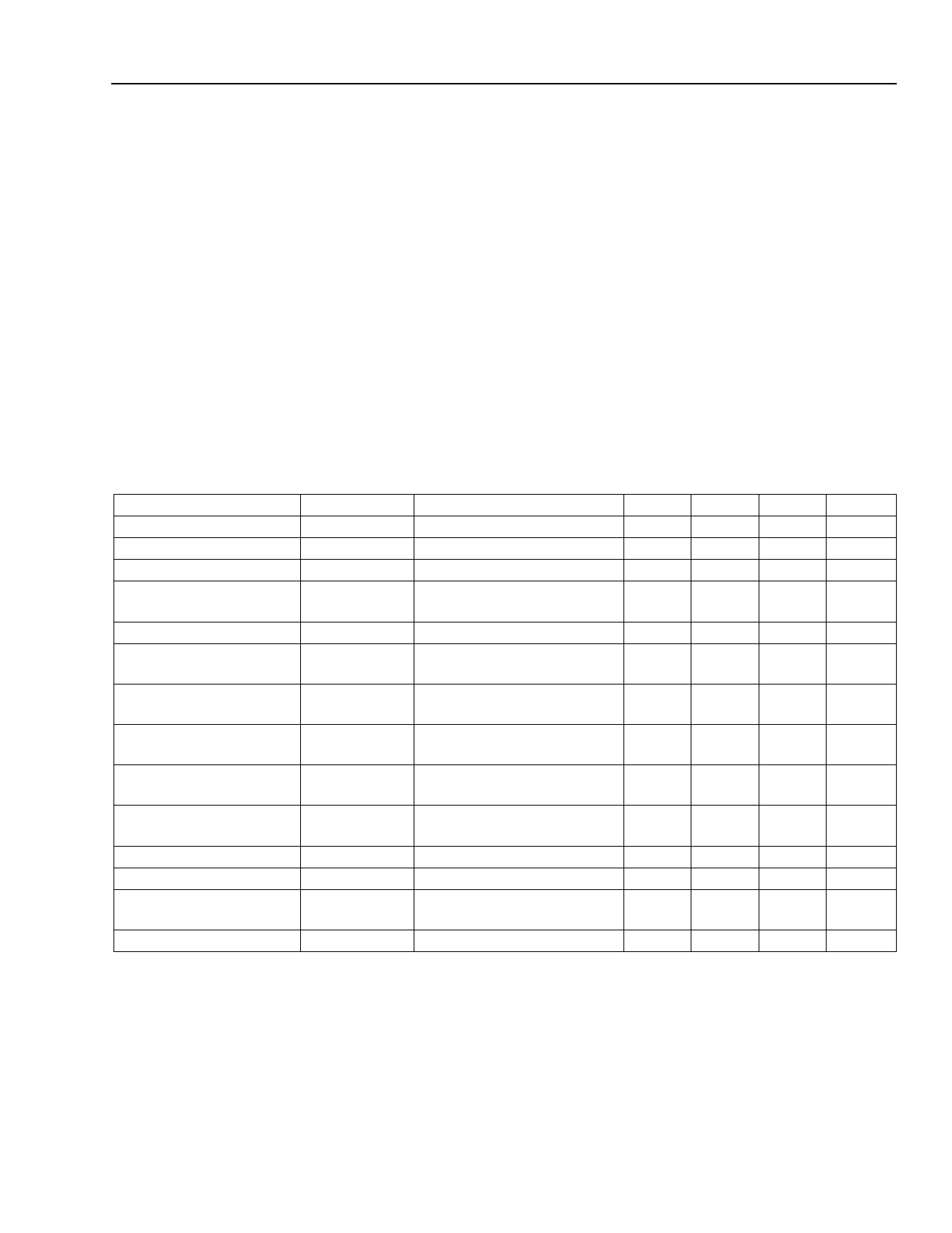
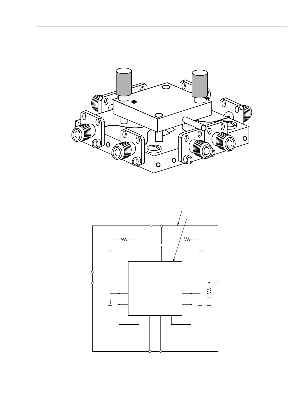
The test fixture mentioned in the data sheet is sold separately and is described in detail below.
Note: Dot on test fixture lid indicates position of pin 1.
Figure 11. TF1003C Test Fixture
5Ω
0.047 µF
V+IN V–IN
FIXTURE BOUNDARY
PACKAGE OUTLINE
5Ω
0.047 µF
12 11 10 9
VBF 13 8
VBR
VBS 14 7
VSS
5Ω
15 6
16 5
1234
5-7208(F).r1
Lucent Technologies Inc.
V+OUT V–OUT
Figure 12. TF1003C Electrical Diagram
5-7209(F)
11
11 Page | ||
| Páginas | Total 12 Páginas | |
| PDF Descargar | [ Datasheet TF1003C.PDF ] | |
Hoja de datos destacado
| Número de pieza | Descripción | Fabricantes |
| TF1003C | LG1605DXB Limiting Amplifier | Agere Systems |
| Número de pieza | Descripción | Fabricantes |
| SLA6805M | High Voltage 3 phase Motor Driver IC. |
Sanken |
| SDC1742 | 12- and 14-Bit Hybrid Synchro / Resolver-to-Digital Converters. |
Analog Devices |
|
DataSheet.es es una pagina web que funciona como un repositorio de manuales o hoja de datos de muchos de los productos más populares, |
| DataSheet.es | 2020 | Privacy Policy | Contacto | Buscar |
